RESEARCH
| |
| Current Areas
of Research
|
| Experimental
Statistical Mechanics |
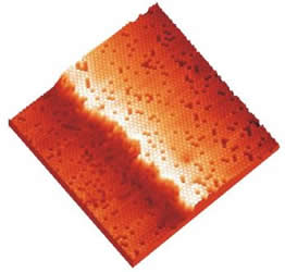 From the
ability to image surfaces with atomic scale resolution follows
the ability to quantify the populations of different structural
features. Of particular interest are the steps that bound
crystalline layers. Because of the low coordination at step
edges, thermal excitations and mass exchange are relatively
easy. As a result, steps play an important role in chemical reactivity
and structural rearrangements. From the
ability to image surfaces with atomic scale resolution follows
the ability to quantify the populations of different structural
features. Of particular interest are the steps that bound
crystalline layers. Because of the low coordination at step
edges, thermal excitations and mass exchange are relatively
easy. As a result, steps play an important role in chemical reactivity
and structural rearrangements.
The spatial wandering of a step and its temporal wandering
under dynamic equilibrium can both be accessed using STM and
other direct imaging tools. Using the tools of classical statistical
mechanics, the measured step behavior is analyzed in terms
of spatial and temporal correlation functions, yielding thermodynamic
free energies and equilibrium time constants. Continuing research issues include
the relationship between the true atomic potential energy
surface and the thermodynamic parameters determined from the
correlation functions, and the experimental signatures of
systems with competing atomic-scale processes. |
 See:
 “Steps on Surfaces: Experiment and Theory,” Surface
Sci. Reports 34, 171-294, 1999, (H.-C. Jeong and E.D.
Williams)
“Steps on Surfaces: Experiment and Theory,” Surface
Sci. Reports 34, 171-294, 1999, (H.-C. Jeong and E.D.
Williams)
Publications list |
|
|
| Pattern
Formation and Structure Evolution |
 |
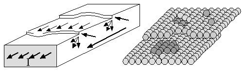
Nanoscale structures,
by virtue of their relatively large surface area, will be
particularly susceptible to thermal decay, and perturbation
by environmental effects. Continuum models of mass transport
will fail for such small structures, but fortunately we can
use the properties of steps to predict nanostructure response.
Basically, we can describe any type of crystalline nanostructure
in terms of the steps that must bound its edges. Then, using
the thermodynamic step parameters discussed above, each step
can be assigned a local chemical potential. This in turn defines
chemical potential gradients that will drive the evolution
of the structure. The time constants for step fluctuations
(also discussed above) then set the time scale for structure
evolution. |
Experimental
applications of this approach to structure evolution on silicon
surfaces, silicon nanostructures and lead crystallites have
confirmed its utility down to length scales of nanometers.
See: Step
Dynamics in Crystal Shape Relaxation
Pattern
Formation Under Electromigration
Publications
list |
|
Statistical Properties of Nanostructures:
Persistence, Electromigration and Noise |
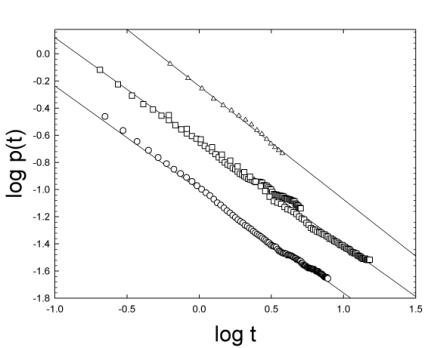 For nanoscale
structures and devices, thermal fluctuations and low probablility
events such as activated nucleation or electromigration biased
mass flow may introduce significant stochasticity into the properties
of interest. Such effects may be manifest as noise, or
as discrete changes in a structural property such as connectedness.
In collaboration with the theory groups of Prof. Das Sarma and
Prof. Rous, the Williams group is investigating the issues of
persistence in step fluctuations and the role of electrical
current in biased surface diffusion. Correlations of noise
with structural fluctuations are under study in collaboration
with the experimental group of Prof. Fuhrer. For nanoscale
structures and devices, thermal fluctuations and low probablility
events such as activated nucleation or electromigration biased
mass flow may introduce significant stochasticity into the properties
of interest. Such effects may be manifest as noise, or
as discrete changes in a structural property such as connectedness.
In collaboration with the theory groups of Prof. Das Sarma and
Prof. Rous, the Williams group is investigating the issues of
persistence in step fluctuations and the role of electrical
current in biased surface diffusion. Correlations of noise
with structural fluctuations are under study in collaboration
with the experimental group of Prof. Fuhrer. |
 See: Persistence
in Step Fluctuations See: Persistence
in Step Fluctuations
“Nanoscale Fluctuations at Solid Surfaces,” Physics
Today 52 24-28 (1999) (Z. Torozckai and E.D. Williams). (Review
Article).
"Experimental Persistence Probability for Fluctuating
Steps," Physical Review Letters 89, 36144-7, 2002
(D.B. Dougherty, I. Lyubinetsky, E.D. Williams, M. Constantin,
C. Dasgupta, and S. Das Sarma).
Publications list |
|
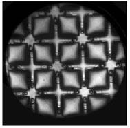
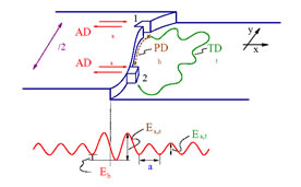
Imaging
Current Flow with Magnetic Force Microscopy
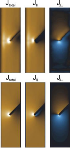 |
The small electromigration force
that causes problems in integrated circuits may become a big
problem in nanostructure devices, where atoms at defects and
surfaces are a larger fraction of the atomic volume. One aspect
of the electromigration problem is that the current flowing
through a structure isn’t necessarily uniform: current
“crowds” into higher density as it flows around
a defect. At small (micron or less) scales, there was previously
no way to measure this crowding effect. We have developed
an application of magnetic force microscopy (MFM) that allows
us to determine the distribution of current flowing around
a defect by measuring the magnetic fields above the structure.
The panels at the left show the measured and calculated current
distributions in a 10-micron wide line with a FIB-fabricated
defect. The current density at the tip of the defect is 4x
as large as the uniform density far away from the defect!
Using this technique, current variations at unknown structures
can be determined – a capability that will be very useful
in diagnostics of electrical connections to nanostructures.
see:
MFM
of Current Crowding
Current Flow around Defect Structures
R. Yongsunthon Ph.D. Dissertation: Magnetic
Force Micrsocopy for Observation of Current Crowding in Electromigration
Phenomena
Publications list
|
|
Analytical
Applications of PEEM
|
Collaborations
| Our research program is strengthened by an extensive network
of collaborations. Much of the collaborative research at the
University of Maryland is carried out within the Nanostructures
Group of the MRSEC. In addition, collaborations with colleagues
at local federal laboratories and international collaborations
are important in our research. |
 |
|
|
Photo Gallery
|
top
|
 |