


Current Flow around Defect Structures
R. Yongsunthon, A. Stanishevsky and E.D. Williams
Materials Research Science and Engineering Center
University of Maryland, College Park
Philip Rous
Department of Physics
University of Maryland, Baltimore County
The metal in electrical wires can actually
be displaced by the flow of electrical current through the wires. This
electromigration-effect is the principle cause of failure in interconnects,
and may dominate the behavior of future nano-scale devices. Mass flow
under electromigration is influenced by the tendency of electrical current
to “bunch” in the region of corners, bends, cracks or materials
defects at the sub-micron size. We have made the first direct observation
of current crowding by exploiting the high spatial resolution available
using magnetic force microscopy. The MFM signature of a fabricated model
defect is shown in the Figure, with the current density obtained by inverting
the image. Away from the defect, the current density is uniform, but the
current deflected around the defect clearly concentrates at the end of
the structure, and there are current “shadows” around the
edges of the defect. Imaging current distributions in this way will allow
hidden defects to be discovered and characterized, and device characteristics
to be quantified in the presence of nanoscale features.
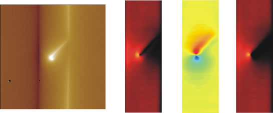
Figure: Left panel - MFM image of 10 micron wide, 0.1 micron thick Au
line, with FIB-fabricated diagonal slit-defect. Current applied is 33
mA. Remaining panels: current density determined by deconvolving the instrumental
broadening and then performing a numerical inversion using the Biot-Savart
Law. The component of the current parallel to line edges is shown in the
second panel, the component perpendicular to the edges in the third panel,
and the net current in the final panel. The decrease of current density
in the “shadow” of the slit is striking, as well as the four-fold
increase in current density within one micron of the end of the defect.