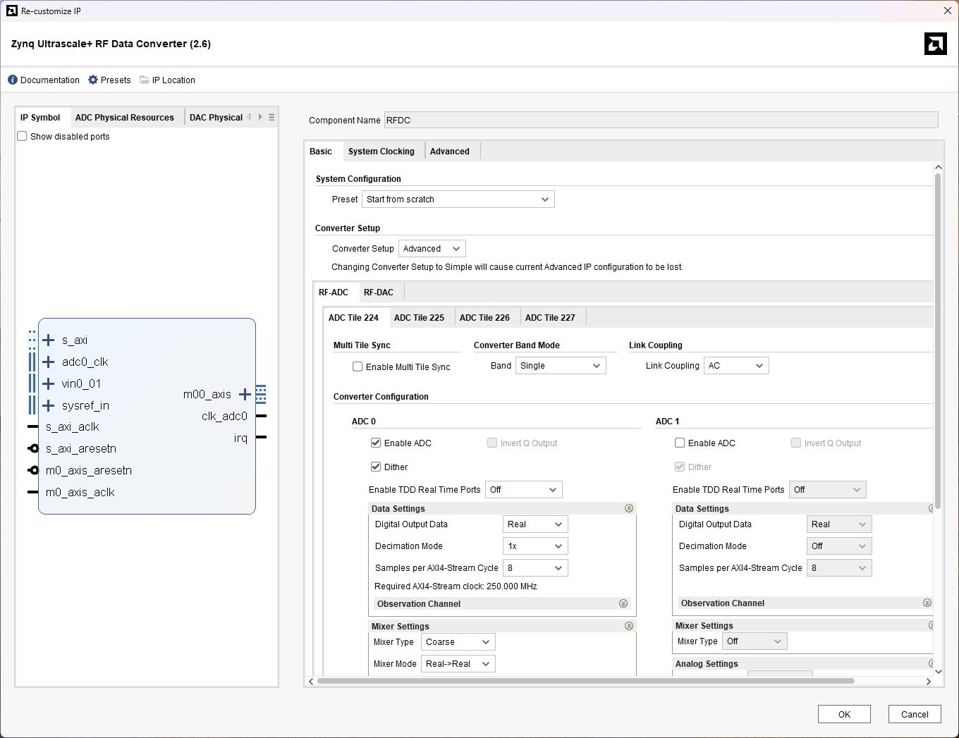
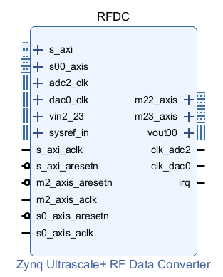
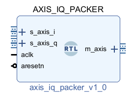
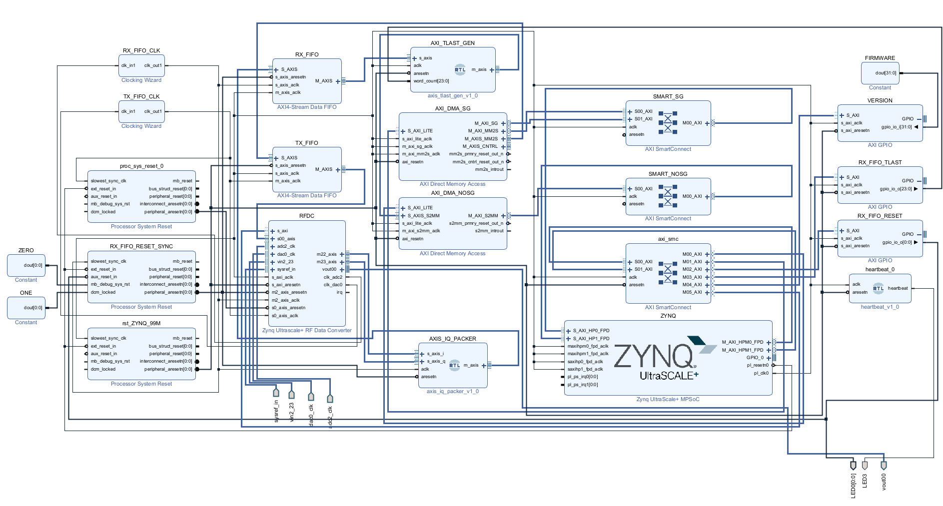
This tutorial shows how to build a project from scratch for the ZYNQ RFSoC that does
the following:
All is controlled from Python with PYNQ, and all filters will be set in the FPGA project
to keep things in the 1st Nyquist zone.
We will use the RealDigital 4x2 RFSoC board running PYNQ version 3.1.1, and Vivado 2024.2. You
should definitely work through the
GPIO and
DMA tutorials first, because we
build directly on them. In particular we re-use the AXI DMA engine and the PS–PL
interface ideas from the DMA tutorial, and assume you are comfortable with the Vivado block
designer, generating a bitstream, and copying the
The point of this project is to do what the canned PYNQ base overlay does not let you
do easily: instead of just programming a static carrier (NCO tone), we feed real, sample-by-sample
I and Q data into the DAC's digital up-converter from a buffer in DDR. That means you can synthesize
any baseband waveform you like in numpy, send it, and recover it.
Back to top
The files needed to recreate everything are here:
Back to top
There are several complications that need to be discussed in order to make such a project work,
notably 1) how to make sure that when we read data from the ADC in Python, we see the signal that
we sent out (also in Python); 2) how to do this using the AXI DMA engines. The former is an
issue of synchronization, and the latter involves details about AXI DMA, a powerful yet also
constrained way to do direct memory access.
First, the synchronization issue. Imagine some python code where you first put some data into
a large array, send it via DMA to the
DAC, route the data from the DAC SMA output into the ADC SMA input, DMA read it back into an
array, and then do something in Python (Fourier analyze, plot, etc). First of all, the DAC in
the RF Converter runs continuously: data in, converted to analog, voltage out. There's no
"start" or "stop" signal. So if you just send a burst
of data to the DAC in the RF Converter, the DAC will immediately process this data and an analog
voltage will appear on the SMA output connector. If you run the cable from this connector
into the ADC, it will do the same thing the DAC does only in reverse: analog in, conversion,
digital data out. No "start" or "stop", continuous operation. But in Python, you want to
make sure that when you read the data from the ADC, you are seeing the waveform that you sent to
the DAC. If you just DMA an array from DDR to the DAC and then read the ADC, you probably
will see only noise unless you control the timing in some way.
The way we will solve this problem is simple: we define an array in DDR memory, and then tell
the hardware to DMA this memory to a FIFO (and we always use a FIFO to cross clock boundaries)
in a mode where when it gets to the last word in the
memory and all the data is transferred, it immediately starts back at the beginning and does it
again, in cyclic mode. This way as long as we read the same amount of data (or less) than we
sent, we will always see the waveform.
There are 2 sub problems with this that we need to take care of. The first involves the
waveform we are sending (waveform wrapping), and the second involves continuity in reading
the FIFO that contains the ADC data (FIFO continuity).
Waveform wrapping
Imagine you want to send a waveform that contains a
sine wave with frequency $f$ and period $T$
on top of some carrier wave (it doesn't matter what frequency). You just build
it in an array in Python, and DMA it in cyclic mode to the FIFO that feeds that DAC.
So you set up a large array with $N$ samples ($N$ is large), and set a "sampling" $f_s$
rate in Python to make the array. When the last
element of the array has been sent, cyclic mode means that the 1st element will follow.
So if the phase between the last element and the first is not continuous, the
discontinuity will generate a spectral leakage tone in the ADC data that
you read back.
To make sure there's no phase discontinuity, first define the buffer length in time
as $T_b = NT_s=N/f_s$ where $T_s=1/f_s$ is the sampling period. Then the number of
wavelengths $m$ of your wave in that buffer time $T_b$ would be given by
$m = T_b/T$, and we want $m$ to be an integer.
Substitute for $T_b=N/f_s$ to get
$$m=N\cdot \frac{f}{f_s}\label{mint}$$
If $m$ is an integer, and $N$ is also an integer by definition, then this means
that $f/f_s$ has to be a rational number.
Note that $f_s$ is
not a free parameter, in fact this is what sets the time scale for your array,
so it has to be related to the true sampling rate of the DAC you will use below,
and the input to that DAC is actually where the true time scale comes from since
that time scale is related to the DAC time scale by the interpolation. As you will
see below, that input rate is carefully calculated, and is the read clock for
the TX_FIFO that sits in front of the DAC. So you have to make $f_s$ equal to
that read clock in order for the definition of time between elements in your array
that you are sending to have a controllable meaning.
Your array size $N$ is probably something you want to specify carefully as well.
If it's an even
power of 2, then that helps with the FFT you might use if you want to send a more
complicated array that comes from an inverse Fourier transform,
and an even power of 2 also helps with the DMA alignment
(DMA bursts are a power of 2, and you want your memory to be an integer multiple
of bursts). So best to make $N$ some even power of 2.
So to satisfy $\ref{mint}$:
and use that in equation $\ref{mint}$ to modify $f$ slightly so that that the ratio
of frequencies is a rational number to get $f'$:
$$f' = \frac{m' f_s}{N}\nonumber$$
As a concrete example, below we have constructed a project that has a TX_FIFO
read clock of 172.032 MHz. We want to generate a tone that has a $f=100$ MHz frequency,
and we will send an array that has $2^{24}=16.7M$ points. If we use those
to calculate $m$ we would get $m=f\cdot N/f_s=100M\cdot 2^{24}/172.032M=9752380.95$.
Turning that into an integer gives $m'=9752389$, and that gives us a value for
$f'=99.99999023$, which is different from $f$ by $\sim 9.8Hz$.
If your waveform is more complex, then you have to work a little harder, but not much.
Say your waveform is generated from a spectrum of frequencies
$f_i$, and you want to inverse Fourier that spectrum and put it into a buffer of
size $N$ that is from a sampling with frequency $f_s$, just like above. Here making
$N$ a power of 2 is even more important for the inverse FFT, and as above you keep
$f_s$ equal to what the hardware requires. So you find $m_i'$ for each $f_i$ such
that $m_i'$ is an integer, and find new frequencies $f_i'$ using $m_i'$ and
equation $\ref{mint}$.
FIFO continuity
This is a problem that has to do with the FIFO that you read for the results of the ADC.
A FIFO means first in, first out, and the usual way a FIFO works, once it's full, it
keeps everything and won't let you write anything more into it. The problem with that
is that the RF Converter will continually send data into the FIFO from the ADC, no
"start" or "stop", as fast as it's supposed to go. Let's say you have a FIFO that is
1024 words deep. If you are not careful, then the first 1024 words will fill the FIFO,
it'll stop, and then when you start reading it, it will allow more data to fill but that
data will be discontinuous from the first 1024 words.
What you have to do then is to control the FIFO carefully by using the FIFO reset
input. What you have to do is to send a signal
(via GPIO) to reset the FIFO, and keep it reset. This prevents any data from
coming into the FIFO from the RF Converter. Then initiate a DMA transfer from
that FIFO. Since the FIFO will be empty, the DMA will wait until it has some data
to transfer. Then you deassert the FIFO reset, and everything will be continuous.
This means you have to first add a GPIO that connects the output to the FIFO reset
input, and write some Python code. But that's all you need to do.
Back to top
Before we start configuring the FPGA and RF Converter, first a little bit on radio
theory might be in order.
Imagine you have 2 waveforms with different frequencies $\omega_1$ and $\omega_2$:
$\cos\omega_1t$ and $\cos\omega_2t$ (but with the same amplitude).
Multiplying these waveforms together is called "mixing" (as understood in the telecommunications
industry), and the math is straightforward, using trigonometry identities:
$$\begin{align}
\cos([\omega_1+\omega_2]t)&=\cos\omega_1t\cos\omega_2t-\sin\omega_1t\sin\omega_2t \nonumber\\
\cos([\omega_1-\omega_2]t)&=\cos\omega_1t\cos\omega_2t+\sin\omega_1t\sin\omega_2t \nonumber\\
\sin([\omega_1+\omega_2]t)&=\sin\omega_1t\cos\omega_2t+\cos\omega_1t\sin\omega_2t\nonumber\\
\sin([\omega_1-\omega_2]t)&=\sin\omega_1t\cos\omega_2t-\cos\omega_1t\sin\omega_2t\nonumber
\end{align}\nonumber$$
Adding and subtracting $\cos([\omega_1+\omega_2]t)$ and $\cos([\omega_1-\omega_2]t)$ gives:
$$\begin{align}
\cos\omega_1t\cos\omega_2t &=\frac{1}{2}\big[\cos([\omega_1-\omega_2]t)+
\cos([\omega_1+\omega_2]t)\big]\label{mixing}\\
\sin\omega_1t\sin\omega_2t&=\frac{1}{2}\big[\cos([\omega_1-\omega_2]t)-
\cos([\omega_1+\omega_2]t)\big]\label{mixing2}\\
\end{align}$$
and adding and subtracting $\sin([\omega_1+\omega_2]t)$ and $\sin([\omega_1-\omega_2]t)$ gives:
$$\begin{align}
\sin\omega_1t\cos\omega_2t &=\frac{1}{2}\big[\sin([\omega_1-\omega_2]t)+
\sin([\omega_1+\omega_2]t)\big]\label{mixing3}\\
\cos\omega_1t\sin\omega_2t&=\frac{1}{2}\big[\sin([\omega_1+\omega_2]t)-
\sin([\omega_1-\omega_2]t)\big]\label{mixing4}\\
\end{align}$$
Equation $\ref{mixing}$ (or any of these equations)
tells us that when you mix 2 waveforms, the result is 2 waveforms,
one which has the difference in frequency and one that has the sum.
The actual multiplying of two analog waveforms together is not a trivial thing,
and for analog waveforms
you might have to build a special circuit using op-amps with matched diodes or
transistors, but it's quite a common thing to do this!
Now let's say you have a wave $\cos\omega t$ (frequency $\omega$) that you want to send,
and you want to send it on a "carrier wave" that has a larger frequency $\omega_0$
($\omega_0\gt\omega$). Say both have the same amplitude.
If the carrier wave is described by $\cos\omega_0t$ and
you mix them together, you will get a transmitted waveform
$$\cos\omega_0t\cos\omega t=\half\cos(\omega_0-\omega)t+\half\cos(\omega_0+\omega)t\nonumber$$
Note that if you mix the $\cos\omega t$ wave with $\sin\omega_0t$ instead of
$\cos\omega_0 t$, you get
$$\sin\omega_0t\cos\omega t=\half\sin(\omega_0-\omega)t+\half\sin(\omega_0+\omega)t\nonumber$$
Here you see clearly that the two transmitted waveforms consist of one with frequency
$\omega_0-\omega$ and one with frequency $\omega_0+\omega$. The terminology is that you are
sending information ($\cos\omega t$) in the "sidebands" of the carrier wave that is centered
at $\omega_0$. What this also means is that the bandwidth needed to transmit information
that consists of the frequency $\omega$ is $(\omega_0+\omega)-(\omega_0-\omega)=2\omega$.
This is not an efficient use of bandwidth!
Let's say the transmitter mixes the incoming $\cos\omega t$ with a carrier wave $\cos\omega_0 t$.
The transmitted wave will then be the product of the signal with the carrier:
$$TX(t)=\cos\omega t\cos\omega_0 t\nonumber$$
The receiver then mixes the incoming signal with a tone from an oscillator that has the same
frequency and phase as the carrier wave: $\cos\omega_0 t$. This gives you
$$\begin{align}
RX(t) &= TX(t)\cos\omega_0 t\nonumber \\
&= (\cos\omega t\cos\omega_0 t)\cos\omega_0 t\nonumber \\
&= \cos\omega t\cos^2\omega_0 t\nonumber \\
&= \half\cos\omega t(1+\cos 2\omega_0 t)\nonumber \\
&= \half\cos\omega t + \half\cos\omega t\cos2\omega_0 t\nonumber \\
&= \half\cos\omega t + \frac{1}{4}\big[ \cos(2\omega_0-\omega)t+\cos(2\omega_0+\omega)t\big]
\end{align}\nonumber$$
You can see in the last step that what you are left with is the original signal $\cos\omega t$
(with half the amplitude) plus a signal centered at $2\omega_0$ with sidebands at
$\pm \omega$. That last part is easily filtered by a low pass filter, leaving only the
signal, at half the amplitude (because you've thrown half of the signal away with the filtering).
Now imagine that you want to send some information to someone over radio frequencies, encoded in
some kind of time varying voltage that's not a simple $\cos\omega t$. For instance,
say the information is of the form $f(t)$, which tells you the voltage as a function of time.
$f(t)$ might be
something simple like the waveform resulting from a microphone output, so the frequency
range will be limited to within a few 10s of kHz. You can mix
$f(t)$ with a carrier wave at a higher frequency, say $\cos\omega_0t$ where $\omega_0$
could be in the MHz radio range, and send all of the Fourier components of $f(t)$ mixed
with $\cos\omega_0t$. The resultant waveform will have the Fourier components of $f(t)$
each mixed with $\cos\omega_0t$, so you will transmit the sum and the difference of each
component with the carrier wave. At the receiver, you then generate the same carrier
wave and mix it with the antenna output, and you will again get 2 waves: the difference,
which will be $f(t)$, and the sum, which will be $f(t)$ mixed with twice the carrier
wave. That higher frequency waveform is easy to filter out, leaving $f(t)$, which is
what you want to send. Such is the power of the principle of superposition!
Voila, you've invented what is called homodyne radio transmission!
(Note: heterodyne radio first mixes the incoming waveform down to an
intermediate frequency (IF), mainly so that you can
filter noise at a lower frequency than the high frequency carrier wave. It does this
by mixing the incoming signal with a wave that has a frequency slightly different
from the carrier wave, filtering the resultant IF waveform, and then mixing with
another waveform that has the IF frequency to get the symbols.)
Back to the simple case of a carrier wave ($\omega_0$) and some information ($\omega$).
The above works if you mix the wave with the information you want
to transmit ($\cos\omega t$) with a carrier wave at the transmitter and the resulting wave
with a carrier wave at the receiver, and both carrier waves have the same phase.
In other words if you mix $\cos\omega t$ with $\cos\omega_0t$ at the transmitter, then
you mix the resulting wave with $\cos\omega_0 t$ at the receiver. And same for if you
use $\sin\omega_0t$, you have to use the same wave at the receiver.
If you don't, and mix the $\cos\omega t$ with $\cos\omega_0t$ at the transmitter:
$$TX(t)=\cos\omega t\cos\omega_0 t\nonumber$$
and $\sin\omega_0t$ at the receiver, you would get:
$$\begin{align}
RX(t)&=TX(t)\sin\omega_0 t\nonumber \\
&=\big[\cos\omega_0 t\cos\omega t\big]\sin\omega_0 t \nonumber \\
&= \cos\omega t\big[\cos\omega_0 t\sin\omega_0 t\big]\nonumber \\
&= \half\cos\omega t\sin 2\omega_0 t\label{cossin}
\end{align}$$
This result eliminates the signal and leaves you with only the high frequency component, which
when you filter out leaves you with nothing. In other words, the relative phase between the
transmitter and receiver carrier wave matters greatly.
So what we really want to do is to construct things so that the receiver is "phase blind" and
doesn't have to know what the phase of the transmitter carrier (whether it's $\sin$ or $\cos$).
We would also like to decrease the required
bandwidth of $2\omega$ for sending a signal at a carrier frequency of $\omega_0$.
So to summarize, we now have 2 problems to solve here:
SSB transmission
Trigonometry is amazing, and the beginnings of the solution to the above 2 problems
was due to an engineer
working at General Electric in the 1940s and 1950s named Donald Norgaard, who pioneered
the phasing method for single sideband communication. He designed
hardware that split an analog signal into 2 paths, one phase shifted by $90^\circ$, and
mixed them with 2 carriers that had a relative phase of $90^\circ$. So we start with a
signal that has 2 phases: an "in-phase" component (I) and a "quadrature" component (Q),
where "in-phase" is relative to the original signal, here $\cos\omega t$.
The information wave would have the form:
$$\begin{align}
I(t)&=\cos\omega t\nonumber \\
Q(t)&=\sin\omega t\nonumber \\
\end{align}\nonumber$$
Then you mix the $I(t)$ component with the $\cos\omega_0 t$ carrier and the $Q(t)$ component
with the $\sin\omega_0 t$ carrier, you would get 2 waves:
$$I(t)\cos\omega_0 t = \cos\omega t\cos\omega_0 t = \half[\cos(\omega_0-\omega)t+\cos(\omega_0+\omega)t]\nonumber$$
and
$$Q(t)\sin\omega_0 t = \sin\omega t\sin\omega_0 t = \half[\cos(\omega_0-\omega)t-\cos(\omega_0+\omega)t]\nonumber$$
and subtract them together to make the transmitted wave $TX(t)$:
$$\begin{align}
TX(t) &=I(t)\cos\omega_0 t-Q(t)\sin\omega_0 t\nonumber\\
&=\cos\omega t\cos\omega_0t-\sin\omega t\sin\omega_0t\nonumber\\
&=\cos(\omega_0+\omega)t\label{iq}
\end{align}$$
By subtracting, we are choosing
the upper sideband $\omega_0 + \omega$. If we were to add we would be choosing the lower
sideband $\omega_0 - \omega$. This is just a convention, both are equally valid, but the
point is that we now are sending only 1 sideband, decreasing the bandwidth needed for
transmission.
This shows clearly that we've already solved problem 1 above: we are now sending a signal
that has a single frequency $\omega_0+\omega$, which means we need a smaller bandwidth
than if we send one with the sum and one with the difference in these two frequencies.
At the receiver, you take this signal and split it into two equal parts by dividing the
power, so each part will have an amplitude:
$$\frac{1}{\sqrt 2}\cos(\omega_0+\omega)t\nonumber$$
Then you mix one of them with $\cos\omega_0 t$ ($I$) and the other with $\sin\omega_0 t$ ($Q$) .
To see this explicitly:
$$\begin{align}
I &= \big[\frac{1}{\sqrt 2}\cos(\omega_0+\omega)t\big]\cos\omega_0 t\nonumber \\
&= \frac{1}{\sqrt 2}\big[\cos\omega t\cos\omega_0t-\sin\omega t\sin\omega_0t\big]\cos\omega_0 t\nonumber\\
&= \frac{1}{\sqrt 2}\big[\cos\omega t\cos^2\omega_0 t - \sin\omega t\sin\omega_0 t\cos\omega_0 t\big]\nonumber\\
&= \frac{1}{\sqrt 2}\big[\half\cos\omega t(1+\cos 2\omega_0t)-\half\sin\omega t\sin 2\omega_0 t\big]\nonumber\\
&= \frac{1}{2\sqrt 2}\big[\cos\omega t+(\cos 2\omega_0 t\cos\omega t-\sin 2\omega_0 t\sin\omega t)\big]\nonumber\\
&= \frac{1}{2\sqrt 2}\big[\cos\omega t+\cos(2\omega_0+\omega)t\big]\nonumber\\
\end{align}\nonumber$$
Voila, we recover the original transmitter $I(t)$ and filter out the higher frequency part near $2\omega_0$.
The other half of the signal is mixed with $\sin\omega_0 t$ at the receiver to get:
$$\begin{align}
Q &= \big[\frac{1}{\sqrt 2}\cos(\omega_0+\omega)t\big]\sin\omega_0 t\nonumber \\
&= \frac{1}{\sqrt 2}\big[\cos\omega t\cos\omega_0t-\sin\omega t\sin\omega_0t\big]\sin\omega_0 t\nonumber\\
&= \frac{1}{\sqrt 2}\big[\cos\omega t\sin\omega_0 t\cos\omega_0 t - \sin\omega t\sin^2\omega_0 t\big]\nonumber\\
&= \frac{1}{\sqrt 2}\big[\half\cos\omega t\sin 2\omega_0 t-\half\sin\omega t(1-\cos 2\omega_0t)\big]\nonumber\\
&= \frac{1}{2\sqrt 2}\big[-\sin\omega t+(\sin 2\omega_0 t\cos\omega t+\cos 2\omega_0 t\sin\omega t)\big]\nonumber\\
&= \frac{1}{2\sqrt 2}\big[-\sin\omega t+\sin(2\omega_0+\omega)t\big]\nonumber\\
\end{align}\nonumber$$
So we recover what we sent.
This is exactly how the ZYNQ RF Converter works, except that it does it in the digital domain.
So far we assumed the receiver's oscillator has exactly the same phase as the transmitter's
carrier. But problem 2 was precisely that the receiver should not have to know that
phase. So let's let the receiver oscillator be off by some unknown phase $\phi$, mixing the
incoming signal with $\cos(\omega_0 t+\phi)$ on the $I$ branch and $\sin(\omega_0 t+\phi)$ on
the $Q$ branch. At the receiver, the steps are identical to above, just carrying $\phi$ along:
$$\begin{align}
I &= \Big[\frac{1}{\sqrt 2}\cos(\omega_0+\omega)t\Big]\cos(\omega_0 t+\phi)\nonumber\\
&= \frac{1}{2\sqrt 2}\big[\cos([\omega_0+\omega+\omega_0]t+\phi)+
\cos([\omega_0+\omega-\omega_0]t-\phi)\big]\nonumber\\
&= \frac{1}{2\sqrt 2}\big[\cos(\omega t-\phi)+\cos((2\omega_0+\omega)t+\phi)\big]\nonumber \\
Q &= \Big[\frac{1}{\sqrt 2}\cos(\omega_0+\omega)t\Big]\sin(\omega_0 t+\phi)\nonumber\\
&= \frac{1}{2\sqrt 2}\big[\sin([\omega_0+\omega+\omega_0]t+\phi)-
\sin([\omega_0+\omega-\omega_0]t-\phi)\big]\nonumber\\
&= \frac{1}{2\sqrt 2}\big[-\sin(\omega t-\phi)+\sin((2\omega_0+\omega)t+\phi)\big]\nonumber
\end{align}\nonumber$$
After the low pass filter removes the terms near $2\omega_0$, the two branches are
$$\begin{align}
I &= \frac{1}{2\sqrt 2}\cos(\omega t-\phi)\nonumber \\
Q &= -\frac{1}{2\sqrt 2}\sin(\omega t-\phi)\nonumber
\end{align}\nonumber$$
Now treat the two branches as the real and imaginary parts of a single complex number,
which is what "$I+iQ$" really means. Recombining (the minus just absorbs the sign flip on the
$Q$ branch we already noted above):
$$I-iQ = \frac{1}{2\sqrt 2}\big[\cos(\omega t-\phi)+i\sin(\omega t-\phi)\big]
= \frac{1}{2\sqrt 2}\,e^{i(\omega t-\phi)}
= \frac{1}{2\sqrt 2}\,e^{i\omega t}\,e^{-i\phi}\nonumber$$
The transmitter sent the complex baseband $e^{i\omega t}$, and we recovered it multiplied by a
constant phasor $e^{-i\phi}$. The unknown receiver phase $\phi$ does not destroy the signal,
it simply rotates the $(I,Q)$ vector by a fixed angle. Contrast this with the
single-mixer case of equation $\ref{cossin}$, where the wrong phase wiped the signal out completely.
And if you care about the signal power, exactly the situation when you're
hunting for an axion conversion signal in ADMX, the phase drops out entirely:
$$I^2+Q^2 = \frac{1}{8}\big[\cos^2(\omega t-\phi)+\sin^2(\omega t-\phi)\big]=\frac{1}{8}\nonumber$$
independent of $\phi$. The receiver is genuinely phase blind: by keeping both
quadratures it recovers the full complex amplitude up to a known rotation, and the power
$I^2+Q^2$ comes out intact regardless of the relative phase between the two oscillators. That solves problem 2.
Back to top
You have a sine wave that has a peak-to-peak range of $V_{pp}$,
and you want to sample it with
an $N$ ADC at some sampling rate. The ADC can return $2^N$ different values,
and each bit of the ADC covers a voltage range of $V_{pp}/2^N$. This is
called the $LSB$.
$$LSB \equiv \frac{V_{pp}}{2^N}\label{LSB}$$
If $V_{pp}=2$ volts
(say the ADC is bipolar between $\pm 1$ volt) and $N_{bits}=8$, then $LSB=2/256=7.8$ mV.
If the output of the ADC returns a value, call this $V_{adc}$ and the signal that gets
sampled is called $V$, then your quantization error is defined as:
$$\delta = \frac{V_{adc}-V}{LSB}\label{qe}$$
Because standard rounding quantizes to the nearest integer of the ADC, this "error"
is really an uncertainty, and is bounded within $\pm 0.5 LSB$, which means
that any value returned by the ADC is only accurate up to half an LSB.
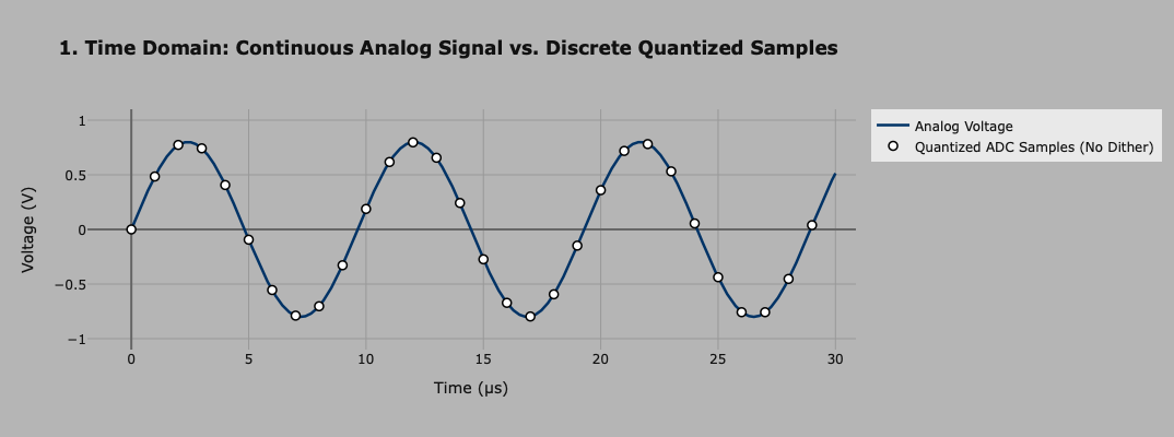
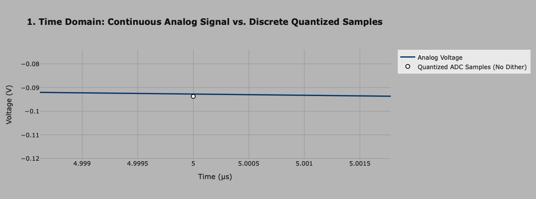
In the following, we plot a $107.3 kHz$ sine wave quantized with an 8-bit ADC,
showing the pure sine wave, and the white sampled points after quantization.
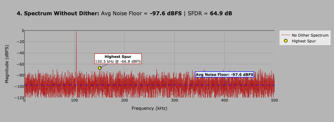
The noise is low, but there are frequencies outside of the main sine wave that
are showing up in the Fourier plot, and that means that those frequencies are
somewhat enhanced. This is a consequence of the quantization, because you
are sampling at a fixed window in time, and the sine wave has a fixed period,
so there will be repeatable places where the quantization error is large. And
that will inject "noise" at a fixed rate, boosting the SFDR. And we might want to
get rid of those "spurs" in the frequency spectrum.
So the way to deal with those spurs is to actually add noise, and do it
in a way that will smear the power of those spurs into adjacent bins, bringing
down the SFDR. But it will add to the noise floor.
Note that we want to add enough noise to the analog signal before
quantization so that the quantization error pushes
the quantized values past digitization boundaries. So if we added noise that
has an RMS of less than 0.5 LSB, it will usually not due a whole log to change
the digitized values from what they would be without dithering,
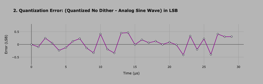
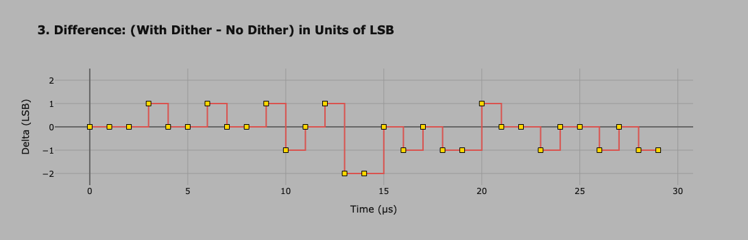
so let's add noise that has an RMS of 0.8 LSB. The effect is shown in the
next plot, where we see the difference between the digital values before and
after dithering.
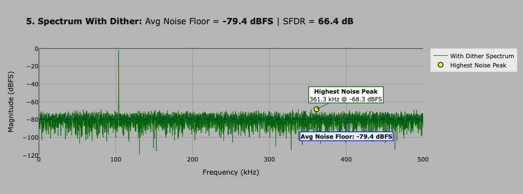
So what did dithering accomplish? It improved SFDR by 1.5 dB, and it
raised the noise floor from -97.6 dBFS to -79.4 dBFS, which looks like we
made the nose 18.2 dB worse. But more importantly, the spur that we see
is not really a spur, it's a noise fluctuation, and it's 11.1 dB above
the noise, as opposed to 30.8 dB, an improvement of over 20 dB. And,
if you do the experiment again, you will find the maximum in a different
place.
When you have an analog signal you want to digitize, and the amplitude is
small compared to the LSB, standard quantization doesn't just create
spurs, but instead turns the continuous sine wave into a harsh square wave or
step function. Just imagine that the amplitude goes below 1 LSB, then it
becomes a flat spectrum, even worse! With amplitude dithering, the noise
constantly bounces the weak signal across the quantization threshold,
and with averaging you can reconstruct the signal wherease without dithering
you will get the signal and a lot of spurs at similar amplitudes.
In applications like radar, you absolutely do not want spurs since you can't
tell those apart from real signals. So dithering is important there.
If the signal is so weak that it's at the same level as the spurs, then you
can't tell the signal from the spur, but dithering will still help if the
signal stays at a fixed frequency and the spurs average out to zero.
With enough averaging the signal will remain.
Back to top
The RFSoC board is basically implementing a digital version of homodyne radio
transmitting and receiving: for transmission (using the DAC), you can supply a
waveform $f(t)$, specify a carrier wave frequency (it will generate the carrier
wave), and it will mix the two together and send it along. For receiving (using
the ADC) you supply the carrier wave frequency and it will mix and filter and
present you with the result.
The RF Data Converter on the ZU48DR (ZYNQ) chip groups 2 ADCs into what they
call a tile, and the same for DACs (2 DACs per tile). This is done to
save resources to some extent, as each of the 2 converters in a tile share the
same clock and PLL resource, but the additional benefit of grouping into a tile
is that because each converter in the tile runs off the same clock and PLL,
they are inherently phase locked, and this can be important when generating
signals or converting analog to digital. Also, the chip allows you to use 2
DACs in a tile to output a complex I and Q waveform, hence phase coherence will
be important. For our purposes, we will only use the DAC to send out real
waveforms.
Tiles that contain ADCs are numbers 224-227 and tiles that contain the DACs
are numbered 228-231. These numbers may seem odd but they are simply the
numbers of the I/O banks the converters connect to on the FPGA, and they are
sequential to keep the clock routing simple (and minimize jitter).
The ADCs and
DACs are referred to by Vivado (2024.2) as "ADC 0" and "ADC 1" on a tile, and
same for the DACs ("DAC 0" and "DAC 1"). If you look at the 4x2 board, you
will see the ADCs and DACs labeled at the SMA connectors with names
ADC_A, ADC_B, ADC_C, ADC_D, DAC_A,
DAC_B. The mapping from SMA label to tile to Vivado label (not an easy
thing to get as it involves quite a bit of cross-checking!) is the following:
The tiles you can use will be 228 and 230 for the DACs (with only 1 DAC
available on each tile), and 224 and 226 for the ADCs (with both ADCs available
on each tile). We will use DAC 0 on tile 228, which means DAC_B on the 4x2
output, and ADC 1 on tile 226, which will mean inputs are on ADC_A on the board.
When we say there are 2 ADCs per tile, by "ADC" we really means a shorthand for
all of the function blocks that go into digitizing an analog signal. And the
same for the 2 DACs per tile, these include all of the digital processing
blocks that result in an analog output.
Both of these are described in the
Zynq UltraScale+ RFSoC RF Data Converter IP product guide (PG269).
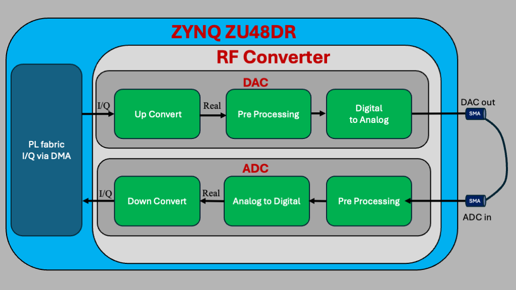
In the following diagram, the RF Converter is shown as a component in the
ZU48DR chip. The block labeled "PL fabric I/Q via DMA" describes the FPGA
parts that lets I and Q data flow via AXI DMA into some FIFOs (not shown), and
from the FIFO injected into the DAC path. The data is first up converted and
mixed to produce a real stream (this is called the "Digital Up Converter", or
DUC stage), and then some processing (filtering) is performed before the
digital signal is converted to analog and sent out to the SMA connector.
We will loop that signal back into one of the ADC SMA connectors, where the analog
signal undergoes some processing, is converted to a digital signal by the ADC
at some sampling rate, and that real digital data stream is mixed and down
converted into a complex I and Q stream and sent into a FIFO for DMA
transmission into memory for the PS to process.
Back to top
Imagine that you want to create an analog output that consists of a carrier
wave with some symbols mixed in. With a ~10 GSps DAC, by the Nyquist theorem
you are limited to carrier waves at 5GHz or less. You could create the I and Q
components in a Python array that lives in the DDR, and DMA the data to the
FPGA and RF Converter and have it added together and digitized by the DAC and
output. But if the DAC is digitizing at 10 GSps, then you'd have to clock your
data in at that rate, and there's no FPGA that can handle data rates that fast.
In fact, try running with a fabric clock above maybe 400 MHz on the ZU48DR and
you will find it difficult to meet timing constraints, which means the design
will be prone to setup/hold violations and the kind of hard-to-debug behavior
(from things like race conditions) that comes with them.
And the same goes for the ADC: digitizing at 5 GSps means I and Q data appear at
that rate, and this is impossible to handle inside the FPGA.
The solution is to "up convert" from the digital data to the sampling rate.
Up conversion is done by the "Digital Up Converter" (DUC) circuit, described next.
Digital Up Converter (DUC)
The DUC's job is actually twofold:
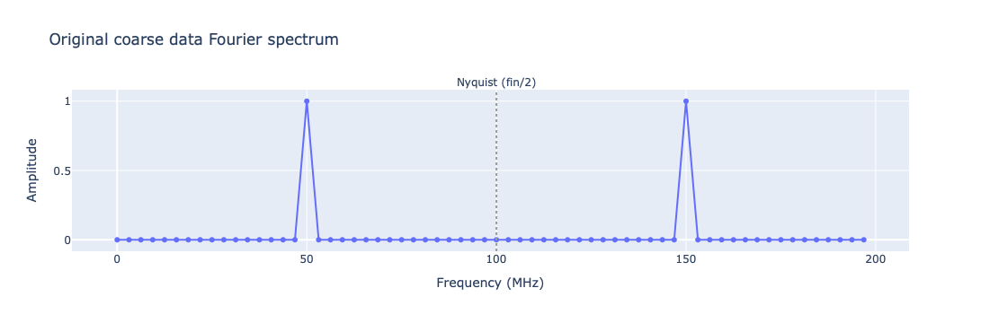
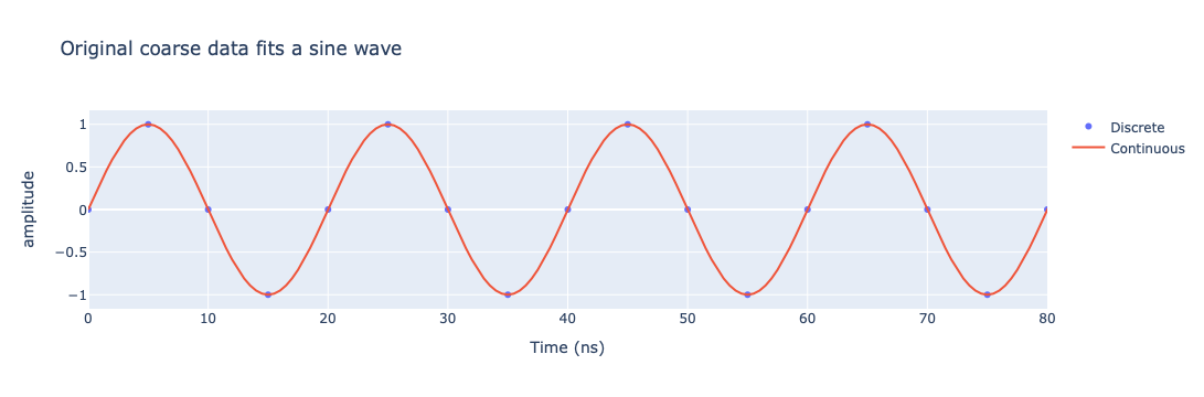
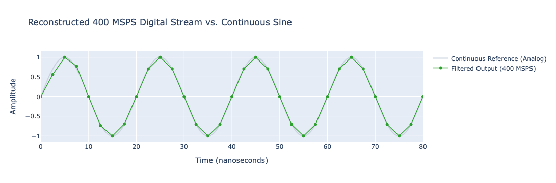
So for example, say you have some data representing a sine wave with a 50MHz
frequency, and you want to convert it to an analog waveform using a DAC running
at 400MSps. We will generate the data at 200MSps, comfortably above the
Nyquist rate for a 50MHz signal, and let the DUC interpolate by 2x to
bring it up to the 400MSps DAC conversion rate. In the figure, the markers show
the coarse 200MSps data sent toward the DAC, and the line shows the sine wave
that these markers fall on. You can see that the period is 20ns=1/50MHz and we
are sending 4 samples per period, which is what a 200MSps data rate gives you.
And the Fourier spectrum will just be a spike in the 1st Nyquist zone. Note
that we are Fourier analyzing the incoming data stream at a sampling rate that
is the incoming data stream rate (200MSps). In the plot below, only the
positive frequencies are shown. We see frequencies in the 1st 2 Nyquist zones:
the 50MHz signal and the image at
200MHz-50MHz=150MHz.
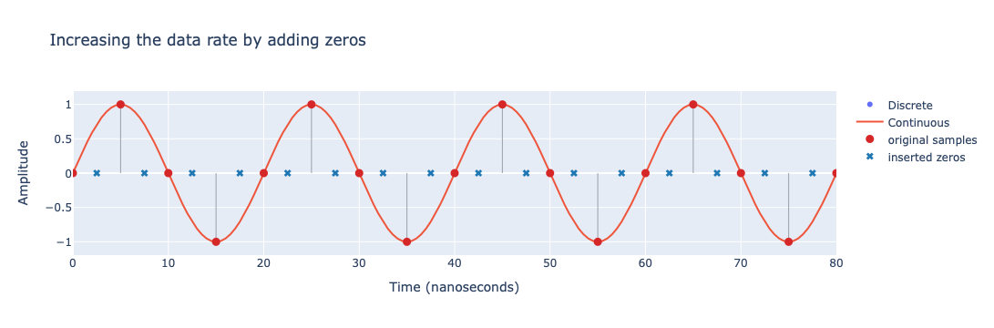
Now for the interpolation. Since you are running the DAC conversion at twice
the rate as the incoming "coarse" data, you need to produce data at twice the
rate that you can feed into the converter. So what the DUC first does in
"interpolating" is to increase the data rate by using each coarse data point
and adding a zero in every other clock cycle. The following plot shows this
new data stream superimposed on the incoming sine wave with the coarse data.
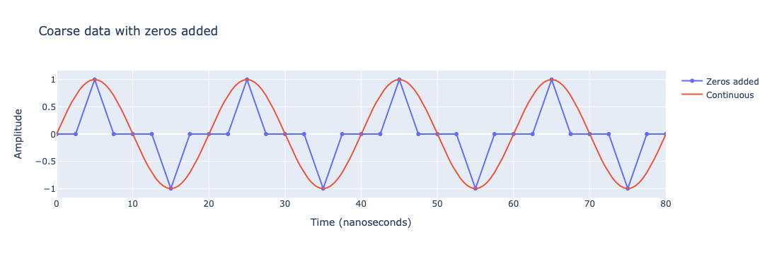
The following plot shows the 50MHz sine wave superimposed on
the coarse data with zeros added:
Since you've added zeros in between each coarse data point, we now have a data
stream with twice the number of points per second, so this is effectively
sampling at twice the rate (and that higher rate is the DAC sampling frequency
we are going to use). Also, those extra zeros mean we now have a data stream
with quite a bit more transitions, so we've effectively added a higher
frequency component to the data.
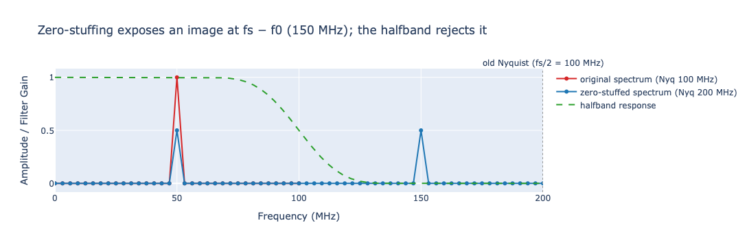
If we Fourier analyze this new data stream, since the rate is twice the rate of
the coarse data, we are "sampling" at a higher rate , and the 1st Nyquist zone
is now twice what it was for the Fourier analysis of the coarse data. The new frequency that shows up is exactly the image of the 50MHz incoming wave in the
2nd Nyquist zone. So by adding zeros you aren't really adding new frequencies,
you are just increasing the sampling rate so that the images show up as
harmonics in the new choppy (zero added) data stream. Having twice the
sampling means that the 1st image from the 50MHz data now falls inside the
analysis band. This is seen in the Fourier plot below:
Zero stuffing allows you to up convert to the DAC sampling rate, but it adds
those higher frequencies. So you have to filter those higher frequencies out.
What the DUC does then is to take the I and Q streams that have been zero
stuffed (we increased the rate by x2, so our "interpolation" is 2), and apply a
filter that filters out everything in the higher Nyquist zones (keeping only
the 1st). This filtering is on each clock cycle of the new double rate data.
For 2x interpolation the filter is a so-called "half-band" FIR,
where FIR stands for "Finite Impulse Response" which describes a filter
that uses a finite amount of the incoming data.
To illustrate, start with an incoming data stream $y[n]$ where $n$ changes
at some rate, and you want to up convert by x2. So conceptually, now you
have an array $z[m]$ where $m$ changes at twice the rate of $n$, and
every other value for $m$ is the zero you've added. You form the FIR
which is a finite array $h[k]$ of size $L$. Now you apply the
FIR to all values of $z[m]$ to make $z_{out}[m]$:
$$z_{out}[m] = \sum_{i=-T}^{T} z[m-i]h[i]\label{FIR}$$
Each element of the filter is called a "tap", which runs from $-T$ to $T$.
The $k=0$ element is called the "center tap", and you set that equal to
1, and every other tap that is an even number away from the center tap is
set to 0. This way, when the filter lands on a non-zero data element,
it just gets copied over as the filter output. When it lands on a
zero element, it then uses the non zero data on either side of that zero
to form the filter output. So a typical half-band FIR with 5 non-zero
coefficient pairs (10), 5 zero pairs (10) plus the center tap,
for a total of 21 taps, and might look like the following:
There are also 3x and 5x interpolation
stages we will meet shortly that don't have this pass-through property, and there,
every output sample is a filtered combination.
Also note that this means that
there will be some delay (latency) inside the DUC due to the fact that it has
to wait to accumulate the data points that come after each sample to use in the
filter.
One more subtlety: stuffing zeros between the samples cuts the amplitude of the
original signal in half, because the signal energy is now shared with
the image. The interpolation filter therefore includes a compensating gain of
2 (a gain of $N_i$ in general for an interpolation factor $N_i$). That's why,
after applying the filter, the data points in the figure below land back on the
original 50MHz sine wave at full amplitude. The new data points fit pretty
well on the original sine wave, as they should. This should not be a surprise:
by applying what is effectively a low pass filter, if it filters out the higher
frequencies then it also smooths out the data.
So the output of the DUC is a smoothed out stream of data that is at the higher
rate: $f_{DAC} = N_i\cdot f_{in}$ where $f_{in}$ is the sample rate of the
data driven into the DUC, $f_{DAC}$ is our DAC conversion rate, and $N_i$ is
our interpolation factor. One caution here: $f_{in}$ is the input sample
rate, which is not necessarily the same as the FPGA fabric clock frequency.
The AXI4-Stream interface into the RF Data Converter normally carries more than
one sample per fabric clock cycle (this is the "samples per AXI4-Stream cycle"
setting in the Vivado IP configuration), so the fabric clock is
$f_{DAC}/(N_i \times W)$ where $W$ is the number of samples per cycle. This is
exactly what makes the high converter rates usable: with, say, 8x interpolation
and 8 samples per cycle, a 6.4 GSps DAC only needs a 100 MHz fabric clock.
Note that the way this is implemented in the ZU48DR is pretty clever. Imagine
that you want to use a large interpolation, like 40x. That would mean a very
large FIR that will have quite a bit more than the 5 data samples on either
side of the non-zero one, and the more samples you have, the more calculations
you have to do, and that means more time and more power. So instead, they
construct filters that only need to do 2x, 3x, 4x, and 5x. Then to get to 40x,
they can apply these filters in series, each time increasing the interpolation
by that factor. So 40x would be from applying 2x, 4x, and 5x in succession.
The ZU48DR can apply up to 3 FIR filters in the last part of the DUC stage,
with the first FIR (FIR1) able to do 2x, 3x, or 4x interpolation, FIR2
can do 2x, 3x, or 5x, and FIR3 can do 2x.
Next in the DAC stage as seen in RF Converter
figure, the output of the DUC is fed into another processing stage. Only now
the output is upconverted, so it is at the DAC converting rate and it is a real
signal with I and Q properly mixed. In the "Pre-processing" stage shown in
that figure, there are 2 things that happen:
Note this means that for the DAC path, if you dial in an interpolation of for
example 20x, and the IMR is in the path, then the full interpolation will be
40x, and Vivado will know this and use it to calculate clock frequencies.
(More on that below.)
The inverse sinc filter is there because of the way the DAC works: for each
data point that arrives in the DAC, the output has to hold that data point for
the duration of the time sample. That means a rectangle in voltage vs time,
and a rectangle in the time domain becomes a sinc wave in the frequency domain.
So the analog frequency response is no longer flat, and this is what the
inverse filter does: compensates so that the output doesn't droop in the 1st
Nyquist zone. (The gen3 DACs also provide a second version of the inverse sinc
filter that flattens the response in the 2nd Nyquist zone, for use with
Mix-Mode described below.)
Finally, the data is fed to the DAC to produce an analog waveform. There
are 2 analog adjustments on chip that can be made:
What Mix-Mode ON allows you to do is to focus power into the 2nd Nyquist
band. And it modifies the inverse sinc filter accordingly. This setting
can be changed inside Vivado (under "Analog Settings" in the DAC configuration
set "Nyquist Zone" to "Zone 2" to enable Mix-Mode)
but it can also be changed in PYNQ. Here's an example:
The VOP adjustment allows you to change the output power by changing the DAC
full-scale output current; the default of 20mA gives about 1 dBm into a 50Ω
SMA connector. On the gen3 parts the VOP feature can in principle adjust the
current over a 2.25 to 40.5mA range, which at the top end would give you
6.5-7.0dBm. But the full range is only available if the board supplies the
DAC_AVTT power rail at 3.0V, and this is a board design choice, not a chip
setting. The RealDigital 4x2 supplies DAC_AVTT at 2.5V (you can verify this in
the board schematics), so the full 40.5mA is not available; for reference, in
the legacy gen1/gen2-compatible output modes, 2.5V on DAC_AVTT corresponds to
20mA operation and 3.0V to 32mA (about 4.5-5dBm). Check the VOP section of
PG269
and the RF-DAC tables in
DS926 for what is achievable at 2.5V before
counting on more than the default output power. A separate consideration is
coupling: the 4x2's DAC outputs go through baluns (AC coupled), which is the
configuration VOP was originally specified for; support for VOP with DC coupled
outputs (over a reduced range) was added in later versions of the rfdc driver.
The ZCU208 board routes the raw DAC outputs to a connector and requires a
breakout card (the XM655) to get to SMA connectors.
The VOP setting can be changed either inside Vivado, or in PYNQ, using
Back to top
Analog
For the ADC path, an analog waveform at the SMA connector goes through
the transformer coupling components (AC coupled) to become a differential signal,
headed to the analog-to-digital converter (ADC). This signal then
enters the "Pre Processing" stage inside the Zynq chip, as seen in the
RF Converter figure.
The ADC on the gen3 ZU48DR expects a 1 volt peak-to-peak (1Vpp) signal,
and since the ADC is bipolar, that means the voltage swings over
$\pm V_{max}=\pm 0.5$V.
For a full-scale sine wave, the RMS voltage is
$V_{rms}=V_{max}/\sqrt{2}=0.35$V, and the corresponding
average power is $P=V_{rms}^2/R=1.25$mW, or $1$dBm.
All of these are specs at the 100Ω differential input to the chip,
where the currents are $I_{rms}=V_{rms}/100\Omega=3.5$mA and
$I_{peak}=V_{peak}/100\Omega=5$mA.
At the SMA connector, which has a 50Ω impedance, the transformer
ideally conserves power, so the same
$1.25$mW gives $V_{rms}=\sqrt{PR}=\sqrt{1.25mW\cdot 50\Omega}=0.25$V,
or $V_{peak}=V_{rms}\sqrt{2}=0.35$V, with currents
$I_{rms}=V_{rms}/50\Omega=5$mA and
$I_{peak}=V_{peak}/50\Omega=7mA$.
This is just the balun's 1:2 impedance step-up at work, going from the
$50\Omega$ SMA to the $100\Omega$ differential input, voltages scale by $\sqrt{2}$
and currents scale down by $\sqrt{2}$ keeping the power fixed.
So at full scale on the ADC pins, given that the transformer coupling is
not completely loseless, you need a bit more than
$1.25$mW at the SMA, but I'm not really sure by how much!
For the RealDigital 4x2 board, there is no active termination, so no
board level protection for over (or under) voltage external to the ZU48DR.
But if you have a signal that has a known bigger voltage swing than what the
ADC is expecting, you can attenuate it
before it hits the ADC using the chip's "Digital Signal Attenuator", or DSA.
It's called "digital" even though it works on an analog input, because you
can configure it with discrete digitally-programmed steps of 1dB between
0 and 27dB.
With the DSA set to 0dB, full scale is limited to the above 1Vpp. Drive past
this and the samples clip, giving you harmonics and a raised noise floor.
Way beyond that and you can damage the chip!
In fact, what the ZU48DR does is to monitor the inputs to the ADC pins,
and if the average power exceeds 14.6 dBm (29mW, or Vpp=4.8V),
it immediately (or as fast as it can) slams in 15dB of attenuation in
the DSA. if the threshold of 14.6 dBm is reached above the
15dB attenuation, the transistors will melt. That would correspond to
a Vpp of around 27 volts at the input to the ADC, or around 19 volts at
the SMA connector. That's pretty good overvoltage protection as you
have to work pretty hard to send that much signal into the 4x2, and
must really want to melt it!
For the ADC path, there is no filtering, and no positive gain, and any
Nyquist zone selection and alias rejection are entirely the responsibility
of who is using the board. The front end "Pre Processing" in the
RF Converter
figure consists of the on-die 100Ω differential termination,
DSA attenuation (signal conditioning)
and over-voltage detection (with flags set in the FPGA
on detection) and protection, and an active differential input buffer to isolate
the input pins from the usual switch-capacitor charge kickback of conversion.
ADC
The analog-to-digital conversion (ADC) channel consists of 8 interleaved ADCs
running at 1/8th of the total sampling rate, sampling the analog input
sequentially, and staggered by 45° in phase. This allows faster
overall sampling, but does introduce gain and time-skew systematics.
To deal with these, the ZU48DR has what are called "Calibration Blocks":
Digital Down Converter (DDC)
Data is now coming out of the ADC at the sampled rate, and as discussed above,
this rate is usually way more than the FPGA fabric can handle. And sometimes
it's way more than the user needs. For our purposes, we will be running the
ADC in complex mode, which means we want what's presented at the output to be
the I and Q quadrature waveforms. So the first thing that the DDC does is to
route the raw digital data, at the sample rate, into the digital mixer, which
multiplies the signal with a complex carrier wave at a frequency $\omega_0$
generated by the
Numerically Controlled Oscillator (NCO, see below). This starts with the
output of the ADC, $x[n]$, and produces $I[n]$ and $Q[n]$ using:
$$\begin{align}
I[n] &= x[n]\cos\omega_0 nT_s\nonumber\\
Q[n] &= -x[n]\sin\omega_0 nT_s\nonumber
\end{align}\nonumber$$
where $n$ is the nth data, and $T_s=1/f_s$, the sampling
period of the ADC.
Decimation and Filtering
The next job of the DDC is to bring the data rate down, and this can be done
easily by throwing away every other data point. Or perhaps doing something
more intelligent, like averaging every 2 higher rate points to make a lower rate
point if the decimation is x2. But there's a problem doing this: imagine
that you are sending data at some carrier frequency into the board, and you
pick your sampling frequency so as to meet the Nyquist condition. But that
there is some noise in the system in the 2nd (or higher) Nyquist zones. For
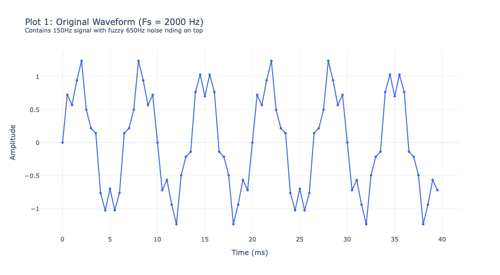
illustration, say you have a signal that consists of a 150MHz sine wave, and
you pick a 2GSps sampling time and a decimation factor of x2. If you average,
or throw away every other data point, that should
give you data that is presented at the output of the RF Converter ADC at
1GSps, your signal is still in the 1st Nyquist zone,
so if you Fourier that waveform, you should see the 150MHz peak.
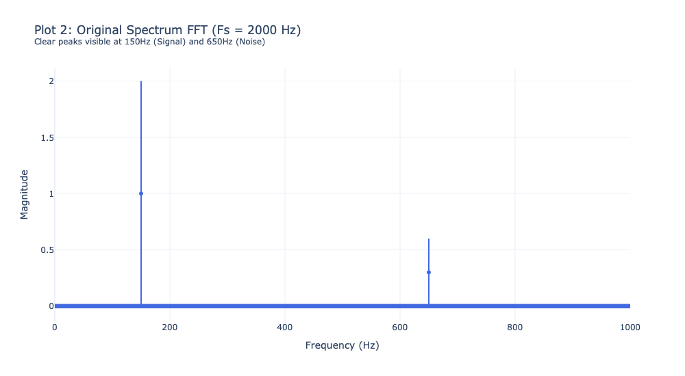
But imagine that you also have some noise that comes from a sine wave at
650MHz with say $30\%$ of the signal amplitude.
Your data looks like this, both waveform and Fourier spectrum:
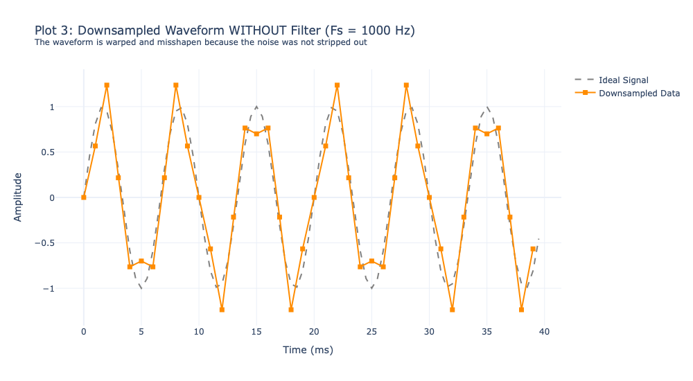
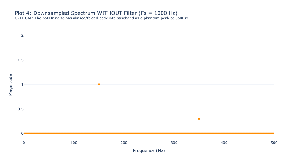
When you decimate, the new
sampling frequency $f_{s_{new}}=\half f_s=1000$MHz, so the new
Nyquist frequency is half that, or $500$MHz. Now your 650MHz
noise is in the new 2nd Nyquist zone, so it is aliased and folds back into
the first Nyquist zone at $f_{s_{new}}-f_{noise}=1000-650=350$MHz.
So to get rid of this, you apply another FIR that effectively decimates
and low pass filters to filter out any energy in the 2nd Nyquist zone of the
decimated signal. This FIR is exactly the same form as for the DUC DAC
path, with the same number of taps, and that makes sense because both need
low pass filters.
For both the DUC (DAC path) and DDC (ADC path), you can dial in various
interplations/decimations in Vivado. These can be 1x, 2x, 3x, 4x, 5x,
6x, 8x, 10x, 12x, 16x, 20x, 24x, and 40x. The way they do this is to
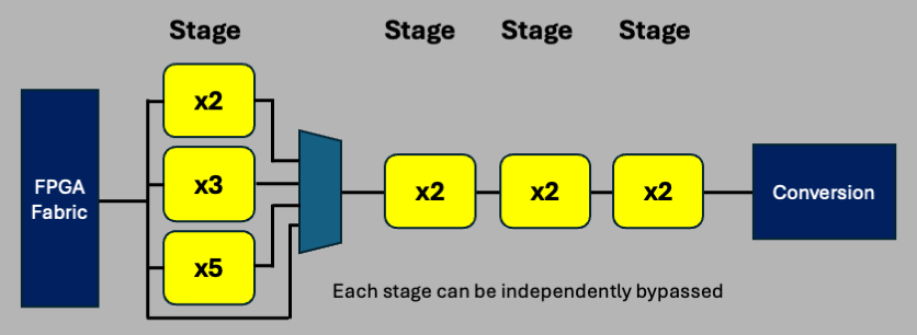
have 2x, 3x, and 5x FIR filters that you can add in 4 stages.
Below is a diagram of what filters are in what stages:
The 2x filter contains 59 taps (29 symmetric pairs plus 1 center tap, or 2x29+1=59),
the 3x filter contains 89 taps (44 + 1), and the 5x filter contains 143 taps
(71 + 1), and the reason the 3x contains more than the 2x can be more easily
understood by thinking about the DUC case, where you have to fill in 2
zeros between data for the 3x interpolation as opposed to 1 zero for the 2x.
So there's more smoothing to do. Same for 5x, it has to fill in 4 zeros
per data, so more coefficients to get a better fit.
This means that for the DUC case (the DAC), the rate is lower at the beginning
of the filter chain, so the filter runs at a slower clock speed, so
the first stage contains either 2x, 3x, or 5x: data runs left to right, from
FPGA to conversion, in
the diagram above. All of the next stages are
2x. For the DDC case (the ADC), the stages are hooked up the same way, only
the data runs right to left in the diagram, and the hardest work is done at the
stage nearest to the FPGA fabric, which runs slower than the conversion side.
One thing to keep in mind: because of the IMR (see above), there's an extra
2x interpolation in the DAC path, which means that you can interpolate up to
80x, but in the ADC path, you are maxed out at the 40x in the FIR filter
path as shown in the diagram above.
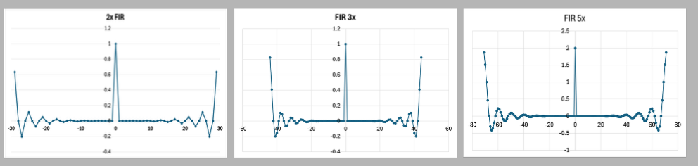
Below are plots of the 3 filters: 2x, 3x, and 5x just to see how these filters
behave. Multiplications inside the DUC and DDC are done digitally, not in
floating point, but these are shown as floating point numbers. The 5x
filter shows coefficients greater than 1 because the filter also has to do
some gain compensation along the way. The main point is to see how these
behave.
Back to top
Each DUC and each DDC in the ZU48DR contains a complex mixer driven by its
own "Numerically Controlled Oscillator", or NCO, which allows you to choose a
programmable digital frequency $f_0$ with 48-bit resolution, with no analog
synthesizer required.
There is also a "coarse" mixer option that mixes at exactly
$f_0=f_s/2$ or $f_0=\pm f_s/4$.
At those special frequencies the local oscillator samples are just $0$ and $\pm 1$,
so the mixer "multiplication" reduces to sign flips and I/Q swaps,
costing essentially no power and introducing zero spurs. To see this explicitly,
note that quadrature functions are sequences of numbers, so
$I(t)\to I[nT_s]$ and $Q(t)\to Q[nT_s]$ where the time $t\to nT_s$
and $T_s = 1/f_s$. If we start with any signal $s(t)$,
then to form $I$ we multiply the signal by:
$$\begin{align}
I[t] &= s(t)\cos(\omega_0 t)\nonumber\\
&= s(nT_s)\cos(2\pi f_0 n/f_s)\nonumber\\
&= s(nT_s)\cos(2\pi \frac{f_s}{2} n/f_s)\nonumber\\
&= s(nT_s)\cos(n\pi)\nonumber\\
&= (-1)^ns(nT_s)\nonumber
\end{align}\nonumber$$
So all the mixer has to do is to flip the sign of every other $s(t)$. It's
also easy to show that $Q[nT_n]=0$ since $Q$ is formed by multiplying by $\sin(\omega_0 t)$.
If you choose $f_0=f_s/4$ we get $I[nT_n]=s(t)\cos(n\pi/2)$ which means
multiplying $s(t)$ by successive $+1, 0, -1, 0$ and repeat. And the same for $Q[nT_n]$.
So there really is no need for any multiplication when using the coarse mixer for
any of these 3 mixing frequencies.
But the coarse mixer only gives you those three fixed frequencies.
For anything else you use the fine mixer and its NCO, described here.
The primary reference is PG269,
Chapter 4, "RF-DAC Mixer with NCO" and "RF-ADC Mixer with NCO".
The NCO is worth understanding: how does it produce a sine and cosine with arbitrary frequencies
without tuning an analog oscillator? The way it works is conceptually simple (with
added complications): imagine a lookup table (LUT) that has $2^{48}$ addresses, and that
lookup table traces out 1 period of a sine wave between $0$ and $2\pi$.
We start with an input $i[t]$ and $q[t]$, and want to form $I[t]=i[t]\cos\omega_0 t$
and $Q[t]=q[t]\sin\omega_0 t$. Now let's say you want to produce
an NCO frequency that is a quarter of the sampling frequency: $f_0=f_{NCO}=f_s/4$.
If you use the LUT values
to sweep out a sine with that value for $f_{NCO}$, you would want to pull out 4 values of the LUT
for each cycle of the NCO. So you define a "Frequency Control Word", or FCW, and set
$FCW=2^{48}/4=2^{46}$,
and define a 48-bit "phase accumulator", ($PA$), that starts at 0, and at each tick of the sampling clock,
you do 2 things:
The NCO frequency $f_{NCO}$ is therefore set by the $FCW$:
$$f_{NCO}=\frac{FCW}{2^{48}}\times f_s\nonumber$$
If on the other hand let's say you would pick a sampling frequency of $9.85 GHz$ (the DAC
maximum) and you would like a carrier wave with $f_0=f_{NCO}=150$MHz. Then solving for $FCW$ gives
$$FCW = \frac{f_{NCO}}{f_s}\times 2^{48} = 4286420965136 = 0x3e602995710\nonumber$$
Any truncation to integer would be off by an exceedingly small fraction of the sampling
frequency, or the frequency resolution, given by
$$\Delta f=\frac{F_s}{2^{48}}\nonumber$$
which at the ZU48DR's 5GSps ADC
rate is about $17.8\mu Hz$ and $35\mu Hz$ at the DAC 9.85GSps rate. You can specify
the NCO value in a Python notebook in the PYNQ environment, and it will actually
allow you to type in a value beyond $\pm F_s/2$ but then will just fold it to the
equivalent alias inside the first Nyquist zone.
This is basically how it works, except that in actuality it employs a few tricks.
For instance, we want the $FCW$ to be 48 bits in order to be able to specify a
very precise
value for the NCO frequency. The actual LUT for the sine wave can be 18 bits
wide with plenty of precision to minimize spurious frequencies (aka spurs).
This makes sense as $2^{48}$ different phases between $0$ and $2\pi$ would be
the definition of overkill!
Also,
the sine wave is very symmetric over the 4 quarters of a cycle, so we only really
need a LUT that has $2^{16}=65536$
entries that span $0$ to $\pi/2$.
Another nice trick: split the 16-bit quarter-wave phase as $\phi = a + b$
with $a$ the top 10 bits, $b$ the bottom 6. Then
$$\sin(a+b)=\sin(a)\cos(b)+\cos(a)\sin(b)\nonumber$$
and since $b=(\pi/2)/2^{10}$ is tiny, expand $\cos(b)\sim 1$ and $\sin(b)\sim b$
to get $\sin(a+b)\sim\sin(a)+b\cos(a)$. So we only need a 10-bit (1024 wide)
LUT for $\sin(a)$, and one small multiply and one add. Storage drops from $\sim 65k$
to $\sim 1k$. They can also use some second-order Taylor expansion tricks to get the
LUT to be even smaller. And as you can imagine, there's an entire industry of tricks
to use, but that's the general idea.
Also note that the $FCW$ is relative to the sampling frequency, which you can set in
Vivado but can also be set in software. So if you set it at one value in the Vivado,
then change it in Python and ask for a particular $NCO$ frequency, it could easily use
the value from Vivado (which it gets from the hwh file). So you should always check it
in Python.
You can also specify the initial phase setting of $PA$ with an 18-bit signed number spanning
$\pm 180^\circ$ giving a phase-offset granularity of
$360^\circ/2^{18}=1.37m^\circ$.
This phase resolution is small, but any subsequent phase
truncation introduces a periodic error in the time domain, which manifests as
a spur in the RF frequency spectrum of the DAC (and ADC), which would add a very
small triangle wave to the waveform. Using the lowest Fourier component of a
triangle wave you can show that the amplitude of any spurious frequency from
phase quantization goes like $6.02\times P$ dBc (dB relative to the carrier
power), and for $P=18$ as it is here, that's a spur that is down by 108 dB
relative to the carrier. Which is quite small. Also, spurs from the
RF Converter's physical imperfections have been measured to be in the
$70-80$ dBc range, so spurs from the phase quantization is $25-35$ dB below
that. This is why 18 bits seems like a
sensible choice for the phase resolution of the NCO.
The 48 bits buy you extraordinarily fine granularity, but the absolute
accuracy and stability of the output frequency are exactly those of the
sampling clock, since $f_{\rm NCO} = ({\rm FCW}/2^{48}) f_s$ inherits every ppm of
error and all the phase noise of $f_s$. On the 4x2 that means the
Si5395 → LMK04828 → LMX2594 chain, and ultimately the 48 MHz crystal
($\pm 25$ ppm or so) unless you feed the board an external 10 MHz reference, as
discussed in the
Clocking section
of the main tutorial. If you care about
absolute frequency calibration, the external reference is what matters; the NCO
adds essentially nothing to the error budget on top of it.
The NCO in the DAC path.
In the DUC, the mixer sits after the interpolation filters, running at the full
DAC rate. For the usual case of an I/Q datapath driving a single real DAC output,
the fine mixer computes
$$y[n] = I[n]\cos(\omega_0 n T_s) - Q[n]\sin(\omega_0 n T_s)
= {\rm Re}\left\{\big(I[n] + jQ[n]\big)e^{+j\omega_0 n T_s}\right\}$$
which is single-sideband upconversion: your baseband I/Q waveform ends up centered
at the NCO frequency $\omega_0/2\pi$. The multiply-and-sum happens inside the mixer
block itself. After the mixer, the (now real) sample stream passes through the
optional QMC block (only relevant if you drive an external analog quadrature
modulator from a DAC pair; irrelevant for direct-RF real output), the optional IMR
image-rejection filter (a final $\times 2$ half-band interpolation, selectable
low-pass or high-pass), the optional inverse sinc filter (compensates the DAC's
zero-order-hold $\sin(x)/x$ droop, with coefficient sets for first or second
Nyquist zone), and then the 14-bit DAC core.
The NCO in the ADC path.
The DDC is the mirror image: the mixer sits immediately after the converter
core, running at the full ADC rate, and before the decimation filters. The
real sample stream $x[n]$ from the ADC fans out to two multipliers:
$$I[n] = x[n]\cos(\omega_0 n T_s), \qquad Q[n] = -x[n]\sin(\omega_0 n T_s)$$
which together form $x[n]\,e^{-j\omega_0 n T_s}$, the complex downconversion.
Park the NCO on your band of interest, and the decimation filters then narrow the
bandwidth and drop the sample rate on both rails before the data crosses to the PL
as an AXI4-Stream. One practical note: if your input signal lives in the second
Nyquist zone (direct RF sampling above $f_s/2$, which is standard practice), the
sampling process spectrally inverts it. Setting the Nyquist zone in the driver
( Setting the NCO from python.
From PYNQ, the NCO lives in the
The frequency and phase registers are double-buffered: writing
Warning: when you set
Quick reference for the NCO parameters (all from PG269 chapter 4 unless noted):
Start
.bit and .hwh files
to the board.
Archive
Project Preamble
Then to make number of cycles $m$ for your tone of frequency $f$ to be an integer:
$$m' = int(\frac{fN}{f_s})\nonumber$$
Radio theory
The solution is in something called "single sideband" transmission, or SSB.
Amplitude Dithering
What the RF Data Converter does
SMA Label Component RFDC Tile Vivado Block
DAC_A DAC 230 DAC 0
DAC_B DAC 228 DAC 0
ADC_A ADC 226 ADC 1
ADC_B ADC 226 ADC 0
ADC_C ADC 224 ADC 1
ADC_D ADC 224 ADC 0
DAC Path


h[-10] = +0.000000 (zero -- half-band)
h[ -9] = +0.003783
h[ -8] = -0.000000 (zero -- half-band)
h[ -7] = -0.019580
h[ -6] = +0.000000 (zero -- half-band)
h[ -5] = +0.061492
h[ -4] = -0.000000 (zero -- half-band)
h[ -3] = -0.165014
h[ -2] = +0.000000 (zero -- half-band)
h[ -1] = +0.619393
h[ +0] = +1.000000 <-- center tap
h[ +1] = +0.619393
h[ +2] = +0.000000 (zero -- half-band)
h[ +3] = -0.165014
h[ +4] = -0.000000 (zero -- half-band)
h[ +5] = +0.061492
h[ +6] = +0.000000 (zero -- half-band)
h[ +7] = -0.019580
h[ +8] = -0.000000 (zero -- half-band)
h[ +9] = +0.003783
h[+10] = +0.000000 (zero -- half-band)
Note that this filter constitutes a delay since it has to buffer 5 data
points as they pass through.
Also, this is a symmetric filter, because an asymmetric filter will mean that
different frequencies will be subject to some phase delay (and therefore
distortion) through the filter. Also, being symmetric,
this reduces hardware costs, because instead of having to do two multiplications
and add:
$$h[-9]\cdot x[n-9] + h[+9]\cdot x[n+9]\nonumber$$
it can do
$$h[9]\cdot (x[n-9]+x[n+9])\nonumber$$
which is a big advantage since multiplication is quite a bit more costly
than addition.
The IMR is there to allow you to shift to the 2nd Nyquist band if you want to,
and it does this by applying another 2x interpolation followed by either a low
pass filter passing the 1st Nyquist band or a high pass filter passing the 2nd
Nyquist band. One thing to be aware of: the IMR is not always in the signal
path. Whether it is active depends on the "Datapath Mode" selected for the DAC
in the Vivado IP configuration (or via the rfdc driver) — in the default
full-DUC datapath mode the IMR is bypassed, and the IMR datapath modes come
with a restriction on the usable input signal bandwidth. See the DAC datapath
modes section of
PG269 for the details of which combinations are allowed.
from pynq import Overlay
import xrfdc
ol = Overlay("base.bit")
# Grab the specific DAC Tile and Block.
# Note: dac_tiles is indexed by absolute tile position, regardless of
# which tiles are enabled in your design:
# dac_tiles[0] = tile 228, dac_tiles[1] = tile 229,
# dac_tiles[2] = tile 230, dac_tiles[3] = tile 231
# On the 4x2 that means DAC_B (tile 228) is dac_tiles[0] and
# DAC_A (tile 230) is dac_tiles[2].
dac_tile = ol.usp_rf_data_converter_0.dac_tiles[0] # DAC_B
dac_block = dac_tile.blocks[0]
# Switch to Mix-Mode (Nyquist Zone 2)
dac_block.NyquistZone = 2
# To maximize power flatness in Zone 2, turn on the inverse sinc filter
# 0 = Disabled, 1 = Zone 1 enabled, 2 = Mix-mode (Zone 2) enabled
# (Check help(dac_block) to confirm the property name your xrfdc
# version exposes for the inverse sinc setting.)
dac_block.InvSincFIR = 2
from pynq import Overlay
import xrfdc
ol = Overlay("base.bit")
# Grab the specific DAC Tile and Block (see the tile indexing note above:
# dac_tiles[0] = tile 228 = DAC_B on the 4x2)
dac_tile = ol.usp_rf_data_converter_0.dac_tiles[0]
dac_block = dac_tile.blocks[0]
# View current structural parameters for the DAC
print(dac_block.OutputCurr)
# Adjust the full-scale output current to attenuate/amplify the signal
# analog-side (value in uA, within the range your board's DAC_AVTT allows)
dac_block.OutputCurr = 32000
#
# Note: it's probably best to check via help(dac_block) to make sure that the
# right value has been entered, and to verify that the value "32" should
# be a raw integer and not a floating point number
ADC Path

Numerically Controlled Oscillator
Then form $I[t] - Q[t]$ and send to the DAC.
NyquistZone = 2) makes the mixer arithmetic account for the flip so
your requested center frequency and sideband orientation come out right; without
it your spectrum appears mirrored.
MixerSettings dictionary of a converter
block. For example, to tune the mixer of ADC tile 0, block 0 to 1500 MHz:
import xrfdc
adc = base.usp_rf_data_converter_0.adc_tiles[0].blocks[0]
adc.MixerSettings['Freq'] = 1500.0 # MHz; sign selects rotation direction
adc.MixerSettings['PhaseOffset'] = 0.0 # degrees, -180 to +180
adc.MixerSettings['EventSource'] = xrfdc.EVNT_SRC_TILE
adc.UpdateEvent(xrfdc.EVENT_MIXER) # latch the new settings
MixerSettings stages the new values, and they take effect on an
"update event" whose source you choose (per-slice, per-tile, SYSREF, etc.). This is
what lets you retune several NCOs and have them all switch on the same clock edge.
Note that with this ordinary update procedure the phase restarts; the frequency
change is not phase-continuous. Gen 3 parts (the ZU48DR is Gen 3) also
support a fast frequency-hopping mode with phase-coherent switching, where multiple
phase accumulators run in the background and a multiplexer selects among them; see
"NCO Frequency Hopping" in PG269 if you need that.
Freq in MHz, the driver converts to an
FCW using the sample rate it believes the tile is running at, and that belief comes
from the hwh file, i.e. from the sample rate you typed into the RF Data
Converter customization dialog in Vivado. Nothing ever measures the actual
clock. The LMX2594 synthesizers that generate the sampling clocks are programmed
independently (by xrfclk), and if they are set to a different rate than
the Vivado configuration declared, every frequency you program will be silently
scaled by the ratio of actual to assumed $f_s$, and every readback will confidently
report the wrong-but-self-consistent number. The Vivado IP setting, the LMX
programming, and your python assumptions are three copies of the same number that
nothing reconciles automatically. Keep them in sync by discipline.
| Parameter | Value | Notes |
|---|---|---|
| Frequency word | 48-bit signed | spans $-f_s/2$ to $+f_s/2$; driver folds requests beyond that to the equivalent alias |
| Frequency resolution | $f_s/2^{48}$ | $\approx 18\ \mu$Hz at 5 GSPS; $\approx 35\ \mu$Hz at 9.85 GSPS |
| Phase offset | 18-bit signed | $\pm 180^\circ$, granularity $360^\circ/2^{18} \approx 1.4$ millidegrees |
| Phase reset | 1 bit | aligns NCO phases across converters; used with MTS |
| Update latch | event source | slice, tile, SYSREF, marker, or PL signal; double-buffered registers |
| Coarse mixer alternative | $f_s/2$, $\pm f_s/4$ | trivial LO values ($0, \pm 1$): no multipliers, no spurs, low power |
| Frequency hopping | Gen 3 | phase-coherent, phase-continuous, or phase-reset switching; see PG269 "NCO Frequency Hopping" |
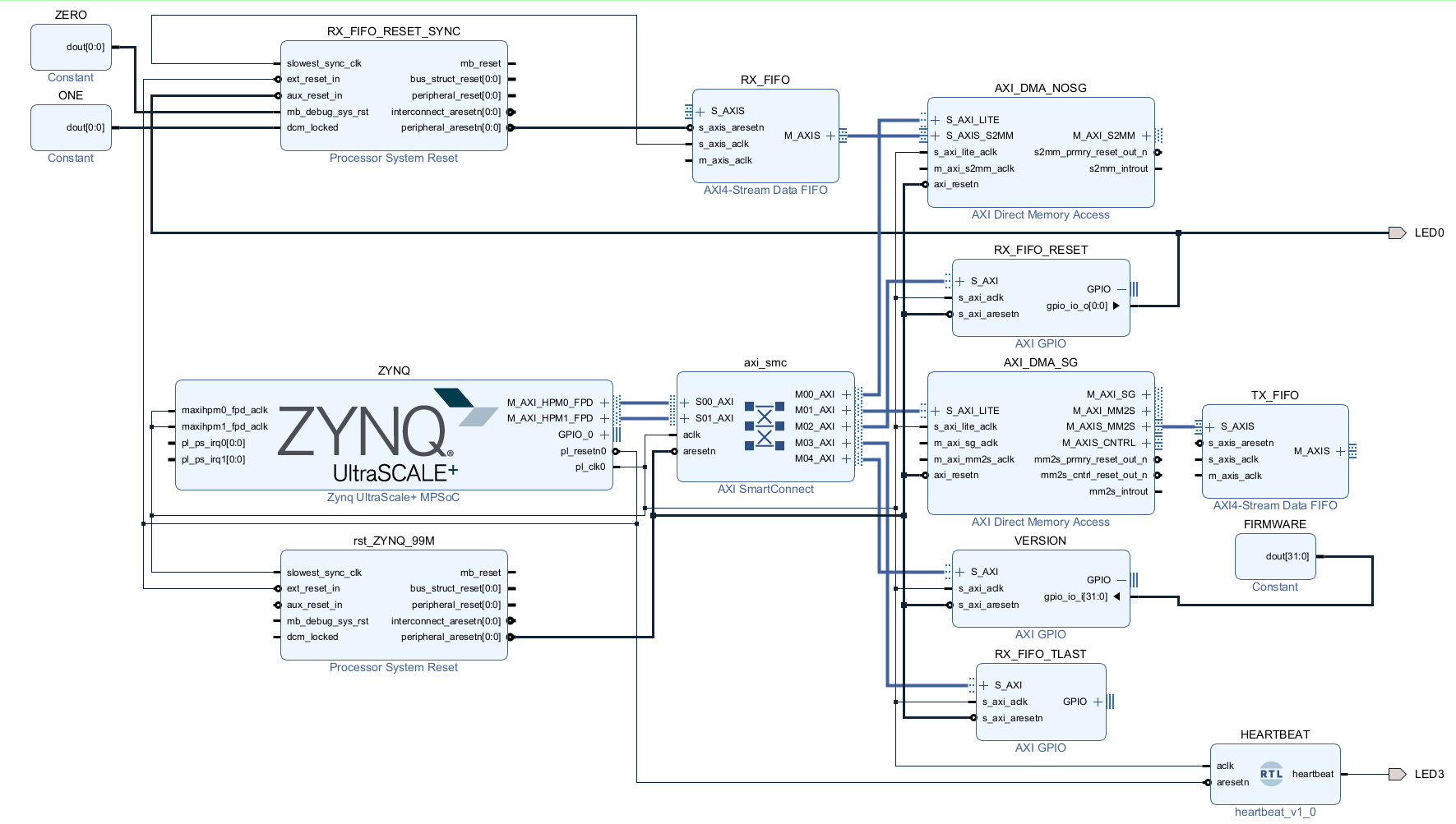
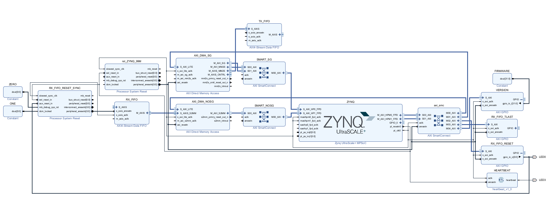
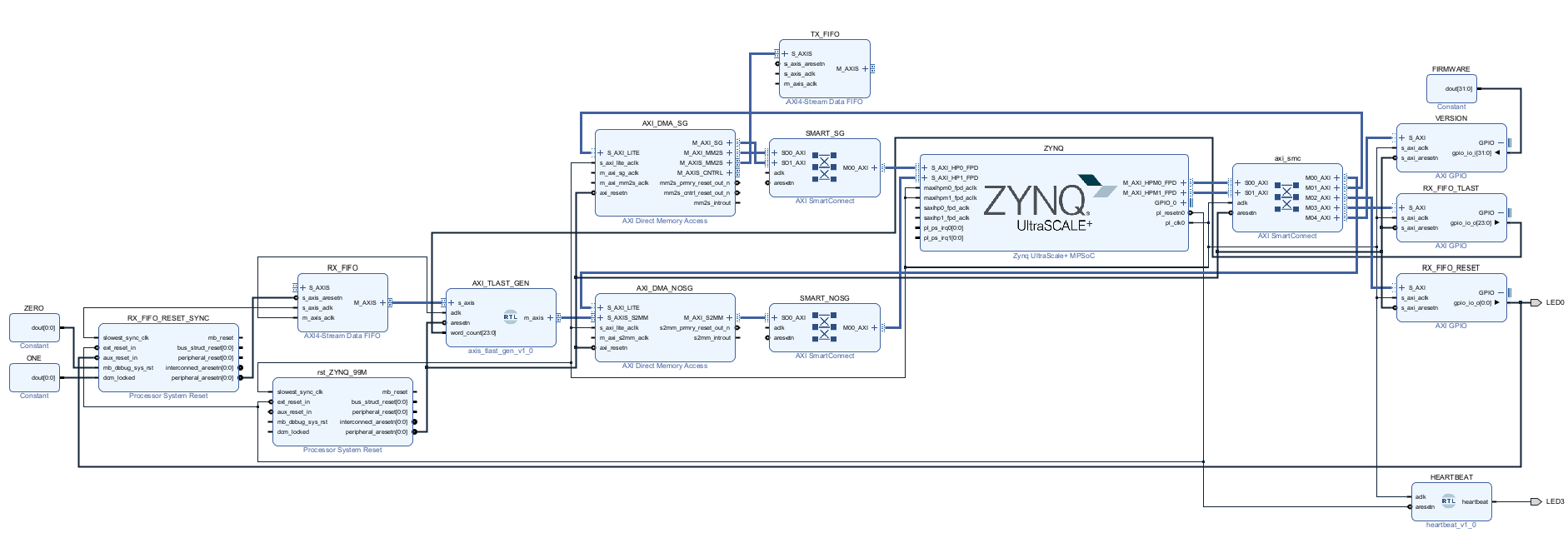
Now we are ready to create the FPGA project. Run Vivado, create a new project, and call it "Loopback_v0x1" since this will be version 2. In "Project Type" make sure "RTL Project" is selected, hit Next, and skip "Add Sources" and "Add Constraints (optional)" by hitting Next twice. That brings you to the "Default Part" window. Assuming you already ran the previous GPIO project, you have the right board files loaded, so click on "Boards" (next to "Parts"), type "4x2" in the Search window, click near the blue title to select the 4x2 board entry, and hit Next, then Finish.
You will now see the usual Vivado windows. On the left, click "Create Block Design", type "Loopback" in the "Design name" window, and hit OK. This brings up an empty "Diagram" window.
Back to topClick the thick "+" in the "Diagram" window, type "ZYNQ" in the Search window, and choose "Zynq UltraScale+ MPSoC" (the ARM processing system, the PS). Do not choose the one with "RF Data Converter" in the title yet, that is a separate IP we will add in a moment. Double click the "MPSoC" entry to drop it in, then click the blue "Run Block Automation" link, leave everything selected, and hit OK. Rename the block to "ZYNQ" in the "Block Properties" window.
While you have the ZYNQ block open, we need to make sure a PL clock is available to clock the
memory-mapped and control sides of our logic. Double click the ZYNQ block, go to the "Clock
Configuration" tab, expand "Output Clocks" → "Low Power Clock Domains"
→ "PL Fabric Clocks", and make sure PL0 is enabled
(100 MHz is fine for now). This "PL0" clock will enable an output port called pl_clk0
on the ZYNQ block, and this port will clock the DMA's AXI4 and AXI4-Lite ports. The fast
sample-rate clocks for the converters come from a completely different place (the on-board clock
chips), which we will get to.
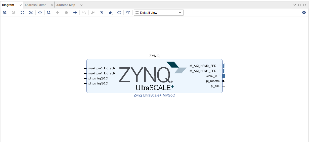
You should see "Run Block Automation" at the top of the "Diagram" window. Click that now. This adds important board preset capability, which configures the DDR4 controller, PS clocking, and wires up the clocks and resets. When you click it, it opens a new window called "Run Block Automation". Make sure "Apply Board Preset" is checked, and everything on the left is checked ("All Automation" etc) and hit OK. You should see this in the Diagram window:

Back to top
Add a constraints file exactly as in the GPIO and DMA tutorials so the bitstream is compressed and
the over-temperature protection is on. In the "Sources" window click the "+" symbol, select
"Add or create constraints", hit Next, click "Create File", call it "Loopback", and click OK, then
Finish. In the sources window, you should see the Constraints change to "Constraints(1)", which
means the new file is there. Expand and you should see
"Loopback.xdc". Double click to open and an editable window should appear to the right,
where you add:
The first 2 constraints compress the bit file and enable over-temperature shutdown features,
and the next 2 set up so that we use the leds on the top left of the board to show a few
interesting things (talked about below).
Save the file (control-s).
Back to top
We want to drive the DAC output with a cyclic DMA, but we want the ADC to be a one
time write into DDR using the RX_FIFO reset to trigger. Cycle vs regular is best
done with 2 different DMA engines, so we will need to add both here:
Add two "AXI Direct Memory Access" blocks exactly as in the DMA tutorial.
One will be for the DDR4 to DAC path, and one will be for the ADC to DDR4 path,
and they will have to be configured differently.
To do this, go back to the Diagram window, click the plus sign to add a block, search for
"AXI DMA", select "AXI Direct Memory Access", and double click. A new block
appears, the title underneath whold be "AXI Direct Memory Access". Then add
another (copy/paste should work but if not, do it by hand).
Name one "AXI_DMA_SG" and the other "AXI_DMA_NOSG" just so we can differentiate in
Python.
AXI_DMA_SG takes data from DDR4 and sends it towards the TX_FIFO, so we want the
MM2S channel enabled, and disable the S2MM channel.
The AXI_DMA_NOSG is the opposite - we are streaming into DDR4 so we want the
S2MM channel enabled and MM2S disabled.
Double click on the AXI_DMA_SG, and you will see both "Enable Read Channel" and "Enable Write Channel" enabled. In the 2024.2 version of Vivado, read and write is with respect to DMA, so MM2S is a read and S2MM is a write. Disabling the "Enable Write Channel" on AXI_DMA_SG disables S2MM, which is what you want, uncheck and click OK. Then double click on AXI_DMA_NOSG and disable the read channel and click OK.
Next we have to configure these 2 DMA enginesTo figure the "AXI_DMA_SG", double click to configure it:
Click OK at the bottom to accept those settings.
For the AXI_DMA_NOSG engine, double click, unselect "Enable Scatter Gather Engine" and
set the "Width of Buffer Length Register" to 26, and disable "Enable Read Channel" since
here we will be writing from the ADC to the DDR4, which is considered a "Write Channel".
Click OK to save.
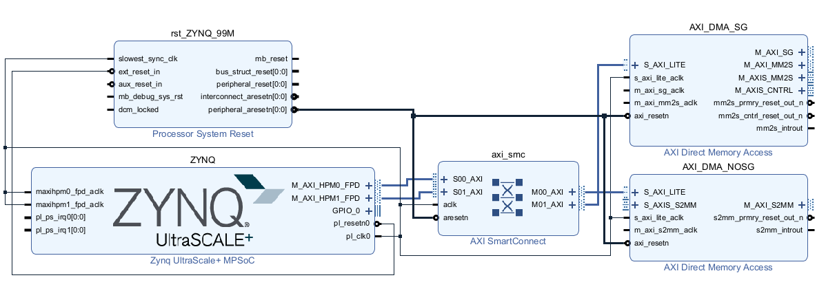
Then click on the "Run Connection Automation" in blue at the top of the
Diagram page. The default should be that all is selected on the left, but if not, select
"All Automation". You should see that both the AXI_DMA_SG and AXI_DMA_NOSG are listed,
and under each is "S_AXI_LITE". This is to hook up the AXI-Lite path, which is for
controls. Hit OK. If after that
you still see a "Run Connection Automation" at the top, do it again, connection automation is
sometimes iterative, and this time it will probably want to hook up the AXI-Lite ports
on the DME engines to the ZYNC (PS) chip. Click OK. Then click
"Regenerate Layout", the button with the clockwise circle at the top of the Diagram page.
The Diagram window should show this:
Probably a good time to save the project.
Back to top
A "heartbeat" is just some way for you to be sure that the FPGA is alive and reasonably
well. One classic way to do this is to just flash one of the LEDs on the board at a
reasonable rate, like 1 Hz, so if it's flashing (the heart is beating) you know it's alive.
We will be setting the FPGA system clock to 250MHz below. To use this clock for a heartbeat,
we will have to slow it down to about 1 Hz. The easiest way to think of how to do this
this is do make a counter that is so large that the MSB toggles at around 1 Hz. If the
system clock is 250MHz, then that clock changes state every 4ns, which means we need
a counter that can count up to around $250\times 10^6$, which means the counter has to be
arond 28 bits. So first let's make a verilog file that will do that:
Create this file somewhere on the PC you are using to build the project and call it
"heartbeat.v".
In Vivado, click the "+" sign to add sources, select "Add or create design sources",
click "Add Files" in the next window, navigate to this new file and select it, and
then make sure "Copy sources into project" is checked. Then hit Finish. You should
see a new file appear under "Design Sources" in the Sources tab.
Now go to the Diagram window, right click, and select "Add Module". You should see
"heartbeat.v" in the list of sources, select it and hit OK. This creates a new block
called "heartbeat_0". Rename it "HEARTBEAT", and connect
"pl_clk0" on ZYNQ to "aclk" on HEARTBEAT, and conenct "aresetn" on HEARTBEAT to
"peripheral_aresetn" on the Processor System Reset block.
Then right click on the Diagram window again
and select "Create Port", give it the name "LED3", set Direction to Output and Type to
Data and hit OK, and connect the "heartbeat" output of HEARTBEAT to this new port.
Back to top
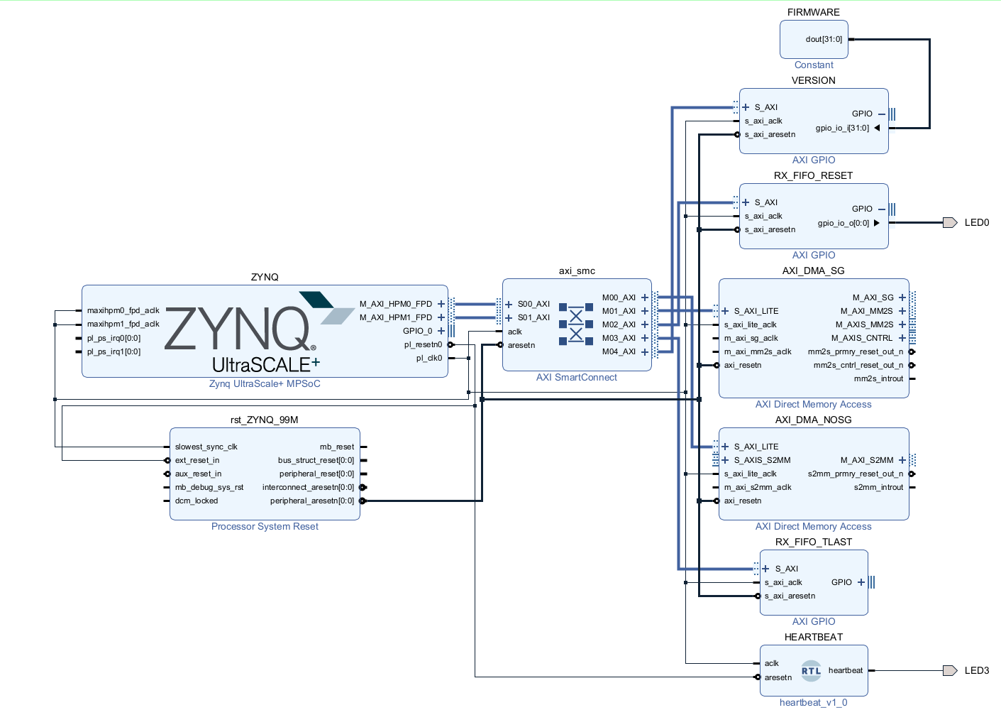
We will need 3 GPIO blocks here:
Double click VERSION and go to the "IP Configuration" tab, and enable "All Inputs".
This makes sure that the inputs are not tristated, but if you don't do it it's ok
because the default tristate is for input. Click OK.
Open the VERSION port "GPIO" so it
shows the 32-bit input
Open the "RX_FIFO_RESET" by double clicking and click on the "IP Configuration" tab. You will
see "GPIO" and "GPIO 2". For GPIO, click "All Outputs" so that it doesn't turn the output
into a tristate, and set "GPIO WIdth" to 1. Notice that the "Default Output Value" will be
0x00000000, which is ok.
Click OK. Then if you open the GPIO port on
that block, you will see it's "gpio_io_o[0:0]" which means it's a 1 bit output.
Note that since the default will be 0, and this will drive the FIFO reset, which is an active
low signal, which means that when the project is loaded, the relevant FIFO will be in reset mode.
In Python we will drive it to 0 for reset and 1 for not reset.
Let's bring this signal out to an LED so that we can see it going on and off. To do that,
right click and "Create Port". That brings up a "Create Port" window. For the "Port name:",
type in the same name as in the last line in the constraint file: "LED0". Change "Direction"
to Output and "Type" to Data and hit OK. Then tie the output of RX_FIFO_RESET to this port.
Next open "RX_FIFO_TLAST", go to the "IP Configuration" tab, select "All Outputs" under GPIO,
and set the "GPIO Width" to 24. This is explained below when we discuss the
TLAST Saga. Hit OK.
Hit "Run Connection Automation", and in the "Run Connection Automation" window, check
"All Automation", but uncheck "GPIO" for RX_FIFO_TLAST,
since will be routing this ourselves, and we don't want Vivado
to route that and have to undo it later, but we do want Vivado to connect these GPIO blocks
to the AXI-Lite bus so that the data gets there ok.
After clicking OK you will still see "Run Connection Automation", but don't run it, it's trying
to connect your GPIO output to something. We will do that ourselves.
Click "Regenerate Layout" (the button with the clockwise arrow in the Diagram window). You should
see something like this:
If your diagram shows any output from the GPIO ports on RX_FIFO_TLAST and RX_FIFO_RESET, don't worry,
just select the output line and any ports that those go to, right click to delete.
Don't forget to periodically save the project.
Back to top
The DMA delivers data from DDR in bursts, but the DAC drains its input at a continuous line rate, so
to keep from starving the DAC at burst boundaries we put in an elastic buffer. The same goes for the
other direction, taking data out of the ADC and writing it into DDR, so we need a buffer
there too, and we will use FIFOs. So click on the "+" to add blocks, and search for "AXI FIFO",
and click on "AXI4-Stream Data FIFO". Careful, not "AXI-Stream FIFO", that's a different beast,
"AXI4-Stream Data FIFO" is the lightweight streaming FIFO, same one we used in
the DMA tutorial.
Double click to add. Then copy and past to add another.
Rename one "TX_FIFO" and the other "RX_FIFO".
The names follow the usual radio convention: TX (transmit) is the outbound path,
where data flows from DDR out to the DAC, and RX (receive) is the inbound path,
where digitized data flows from the ADC back into DDR. Lining that up with the DMA (whose "read" and
"write" are both with respect to DDR): TX_FIFO sits in the MM2S path (DMA reads DDR,
streams out), so its output feeds the DAC input of the RF converter. RX_FIFO sits in the
S2MM path (DMA writes DDR), so its input is driven by the ADC output of the converter.
For each FIFO, double click and make the following changes in the "Re-customize IP" window:
Each FIFO has an S_AXIS port and an M_AXIS port. TX_FIFO is the transmitting data into
the DAC, and that will be cyclic so we will use AXI_DMA_SG.
So the TX_FIFO S_AXIS port connects to the M_AXIS_MM2S port on the AXI_DMA_SG block,
and the TX_FIFO M_AXIS port will connect to the right port on the RF Converter (see below).
For the RX_FIFO, it is sending data from the ADC to the DDR, no cyclic, so it goes through
AXI_DMA_NOSG, so you connect the
M_AXIS port on RX_FIFO to the S_AXIS_S2MM port on AXI_DMA_NOSG, and you connect the
S_AXIS port on RF_FIFO to the right port on the RF Converter to accept data from
the ADC (see below).
So the next thing to do is to make these connections:
Now let's connect the RX_FIFO_RESET line to the RX_FIFO reset. We could just
connect the line by hand, but there's another consideration: a FIFO is a very
synchronous object (that is, it does things by clock) whereas GPIO is
asynchronous (it does things whenever you tell it via GPIO, which is not
necessarily synchronous with any clocks). So we should take care. Now, when
we issue the reset, that will clear the FIFO and prevent any new data from
entering. So we don't have to worry about anything being synchronous. But
when we release the reset, the FIFO will start up, and we don't want
that to happen near the clock edge or we could get race conditions, which
different flip-flops might change differently, which generates unknown effects.
So we are going to have to synchronize our GPIO with the RX_FIFO write clock
(which we will get to later), because that's the clock that defines
"t=0" in the FIFO.
The way to do this is to instantiate a new block called "Processor System Reset".
(These are already in the project, wired in when you hit "Run Connection Automation"
for the ZYNQ block but this one you will instantiate will be it's own and not
used for anything else.) Click on "+" in the Diagram window and type "Processor
System Reset", double click, and rename it to "RX_FIFO_RESET_SYNC".
Then connect the following signals from "RX_FIFO_RESET_SYNC" to "RX_FIFO":
What this block is built to do is precisely what we need: at the rising edge
of "slowest_sync_clk", "peripheral_aresetn" follows "aux_reset_in". So it's
basically just a flip-flop. Here's the timing diagram, below. Remember,
the thing we want to be sure of is that when the GPIO transitions from 0 to
1, that's the release of the FIFO reset, and we want to be sure that that line
is synchronous with the clock.
There's two more lines to connect on the "RX_FIFO_RESET_SYNC" block: the line
"dcm_locked" has to be set to 1 and "mb_debug_sys_rst" set to 0. The former
is the signal that says the input clock is good, but there's no way to generate
that since that clock will come from the RF Converter, so we set it to 1.
The latter is a reset that we won't be using, so set it to zero. To do this,
you instantiate 2 "Constant" blocks, rename one of them "ZERO" and the other "ONE",
set the width to 1 bit and "ZERO" to 0 and "ONE" to 1 and tie them in.
Go ahead and hit the "Run Connection Automation" link at the top. If you've
followed without any mistakes or omissions, you should see the options are to
connect RX_FIFO/m_axis_aclk, RX_FIFO_RESET_SYNC/slowest_sync_clk, RX_FIFO_TLAST/GPIO,
and TX_FIFO/s_axis_aclk. All of these are going to be connected by hand, so
you don't want Vivado to route them because then you just have to undo it.
If you have any other options, then probably it's ok to enable them and let
Vivado route it, so it OK. But if not, then hit Cancel.
Hit the "Regenerate Layout" button. You should see a block diagram that looks
like this:
Back to top
Next we want to enable the ports on the PS (the ZYNQ block) so we can do DMA from the
DDR4 to the AXI_DMA engine, and we should increase the FPGA fabric clock so that we
are sure we are reading the RX_FIFO faster than we are writing it, just to leave us
some comfort!.
Double click on the ZYNQ block (it's the one with
"Zynq UltraScale+ MPSoC" caption), and that opens up the "Re-customize IP" window.
We will follow what we did in more detail in the
DMA tutorial.
Click "PS-PL Configuration" on the left, then expand "PS-PL Interfaces" on the right,
then expand "Slave Interfaces" and "AXI HP". Enable "AXI HP0 FPD" and "AXI HP1 FPD".
If you expand each one of those, it should show that the data width is 128, change them
both to 32. This is probably not necessary, as the hardware will convert, but let's
make things easier for it.
Next, to change the clock speed,
click on "Clock Configuration" on the left, select the "Output Clocks" tab,
and expand "Low Power Domain Clocks" and then "PL Fabric Clocks". You should see
"PL0" checked, so change "100" to "250".
Click OK, and again don't hit the "Run Connection Automation". We will be routing
what's left by hand (below).
The block for ZYNQ should change to show 2 new ports: "S_AXI_HP0_FPD" and
"S_AXI_HP1_FPD", both coming out of the top left corner of the ZYNQ block.
Back to top
Now we want to connect the AXI bus (not the AXIS stream side!) lines between the
ZYNQ ports we just made and the AXI_DMA ports. And there are actually 3 ports
on the AXI_DMA block that we need to connect: M_AXI_SG (gets scatter-gather info),
M_AXI_MM2S (grabs data from DDR and sends it to the TX_FIFO), and
M_AXI_S2MM (takes data from RX_FIFO and sends it to DDR).
So there are 3 AXI master ports on AXI_DMA and 2 AXI slave ports on the PS to access
DDR. Since AXI is a complicated thing, we always want to route lines from master
to slave on AXI through an AXI Smartconnect block. This block will handle all of the
conversions necessary, and keeps things in order.
So back to the Diagram, click "+" and search for Smartconnect,
and add 2 "AXI SmartConnect" blocks.
Open up one of them and in the configuration, change "Number of Slave Interfaces" to
1 and hit OK, and rename that block "SMART_NOSG". Rename the other AXI Smartconnect
to "SMART_SG", and make sure it has 2 slave ports.
The MM2S direction is where the AXI_DMA_SG engine pulls data from DDR4 and sends
it into the RFDC DAC input,
cycling. So that one will have the MM2S direction and the scatter-gather ports
on AXI_DMA_SG. AXI_DMA_NOSG will connect to SMART_NOMSG. So make
the connections that are outlined in the following table. And be careful to connect
M_AXI_* and not M_AXIS_*, we are connecting on the AXI DDR side of the DMA engine!
Don't "Run Connection Automation", as we are not finished connecting things by hand!
Hit "Regenerate Layout". Your block diagram should now look something like this:
This would be a good time to save the project.
Back to top
Before working on the RF Converter, there's one more issue. When we want to
read data from the RX_FIFO into DDR4, we ask the DMA engine to to initiate the
transfer, all through Python. So the code knows the size of the buffer, but
this size is really a maximum as far as the DMA goes: don't send more than this
into the buffer. But the DMA engine is not counting data that gets sent, it's
only sending data to the DDR4 using the AXI protocols, which involve the following
control signals:
Data only moves across the bus when both TVALID and TREADY are
high at the same time. This is how they "handshake".
The problem is, who sends TLAST? For the transfer from DDR4 to the
AXI DMA engine to the TX_FIFO to the DAC, the AXI DMA engine itself
generates TLAST. But when data goes the other way, from the FIFO into
the DMA engine, there's no way to know how much data to then send into the
DDR4. So no one generates TLAST and the system hangs.
But TLAST is known by the system and actually is sent to the DMA engine on
the AXI_LITE bus as a slow contorl. So we will have to make our own module
that sits in series between the RX_FIFO M_AXIS port and the AXI_DMA
S_AXIS_S2MM port that gets this information, and when the transfer starts,
counts, and asserts TLAST when it's done.
Here's some
verilog code that does the trick:
"DATA_WIDTH = 32" is the width of the AXIS bus and the AXI bus. This has to match!
Also, "COUNT_WIDTH = 24" matches what we put into the DMA engine configuration when we set
"Width of Buffer Length Register" to 26, the maximum. This matches, because if we send
$2^{24}$ words each of which is 32 bits, or 4 bytes, that's $2^{26}$ bytes which is
what "CNT_WIDTH" means.
Copy this file to the PC you are using
to build the project. Then go into
the "Sources" window in Vivado, click the "+" sign to Add Sources, and select
"Add or create design sources" and hit Next. Then click "Add File" and it brings
up a file browser, find the source file axis_tlast_gen.v and select it. Then
in the window "Add Sources" check the box that says "Copy sources into project".
Then hit Finish. This should add "axis_tlast_gen" at the same level as
"Loopback" in the "Design Sources" line of the Sources window.
Now we want to turn that into a block module. So go back to the diagram
canvas and right click and select "Add Module".
It should bring up a window called "Add Module" and it should have
"axis_tlast_gen (axis_tlast_gen.v)" selected. Hit OK, and it should
instantiate a new module in the Diagram window that is unconnected to
everything already there. Rename it "AXI_TLAST_GEN". It should look like this:
The first think to do is to delete the connection between RX_FIFO "M_AXIS"
and AXI_DMA_NOSG "S_AXIS_S2MM", which is the output of the RX_FIFO into the AXI_DMA_NOSG
engine. Select the line, right click, and delete. We want the output of
RX_FIFO to go into the AXI_TLAST_GEN module so it can count the number of
words sent, and we want all of that AXI stream to just pass through. So the
RX_FIFO "M_AXIS" goes into AXI_TLAST_GEN "s_axis" port, and we want the
"m_axis" output of AXI_TLAST_GEN to go into the AXI_DMA_NOSG "S_AXIS_S2MM" port.
Connect them up.
Next open up the GPIO port on RX_FIFO_TLAST and connect
"gpio_io_o[23:0]"
to "word_count" on AXI_TLAST_GEN so it knows how many to count. And connect
"aresetn" on AXI_TLAST_GEN to the "s_axi_resetn" port on any of the GPIO blocks.
And lastly, connect "aclk" on AXI_TLAST_GEN to "m_axis_aclk" on the RX_FIFO
block, because remember axis_tlast_gen is counting words that come out
of the RX_FIFO and into the AXI_DMA block, so we want to count with
the same clock. Note that neither of these drives that clock, that will be
dealt with in the RF Converter Configuration section below.
Hit the "Regenerate Layout" button. But still, don't hit "Run Connection Automation",
we have more to connect by hand!
Your diagram should look like this (although at this point it might be
difficult to see details, the topology should be the same).
At this point, all we have left to do is instantiate the RF Converter,
configure it, and make sure we know what clocks we want to employ and
connect them up to the relevant FIFO ports that connect into the RF Converter.
Now would be a good time to save the project!
Back to top
Click the "+" button in the block design window to add another IP, search for ZYNQ and add
"Zynq Ultrascale+ RF Data Converter". Change the name to "RFDC" in the "Block Properties"
window.
Note that the "Run Block Automation" and "Run Connection Automation" links are still
there, which is good. The "Run Block Automation" is for the RFDC that you just
instantiated, it sets it with what works with the RealDigital 4x2 board. So this should
be run first. But it's safer to first configure the RF Converter for the ADCs and
DACs you want to use, before "Run Block Automation" just to be sure it doesn't
configure something you have to change later.
Double click on the RFDC module you just instantiated. It will bring up a window
that will look like this:
You will see that the "RF-ADC" tab is selected, and you see the 4 tiles 224, 225, 226, and
227 are tabbed below. Let's use "ADC_A" on our 4x2 board, and that input is connected
to "ADC 1" of tile 226, so unselect "Enable ADC" under "ADC Tile 224", then click
on "ADC Tile 226" and click "Enable ADC" under "ADC 1".
Next click on "RF-DAC".
Let's enable the "DAC 0" in tile 228, and that one comes out the "DAC_B" SMA connector on
the 4x2. So click on "tile 226" and enable "DAC 0", and make sure "DAC 1" on that tile and
no other DACs are enabled (they shouldn't be). Then hit "OK". This will change the
RFDC block, which should now look like this:
You will see these inputs and outputs:
On these inputs and outputs,
the "s_" and "m_" prefixes refer to "slave" and "master", and this is from the point
of view of the RFDC block relative to the FPGA fabric.
So "m_" means that the RFDC drives it, meaning an ADC conversion of the
analog input that delivers digital data from the ADC
out of the RFDC into the FPGA. "s_" means
that the FPGA sends data into the RFDC so that it can convert it at the DAC
to an analog output.
System Clocking
Double click RFDC again and select the "System Clocking" tab. This is probably
the most complex part of the project, so let's go slow.
First, at the top you should see "AXI4-Lite Interface Configuration" and under
that, "AXI4-Lite Clock (MHz)" set to 100. Change that to 250, since we are going
to be running the FPGA fabric with that clock. Hit OK, and connect "s_axi_aclk"
on the RFDC to any "aclk", which should come out of the "pl_clk0" port on the ZYNQ block.
Next double click RFDC again and go back to the "System Clocking" tab. We are
using the ADC from Tile 226 and the DAC from Tile 228, so check "PLL" in the
table for both of those rows. Notice that the "Sampling Rate (GSPS)" column shows
2.0 for Tile 226 and 6.4 for Tile 228 (or maybe other random numbers),
but we will change those.
When you select "PLL" for each Tiles 226 and 228, it calculates a reference clock
such that the sampling rate will be a multiple of it, and you will see maybe
250 for row "ADC 226"
and 400 for "DAC 228". What we have to do first is set the sampling rates, and then
everything flows from those numbers.
Note that as discussed in the
clocking
section of the
RFSoC introduction,
on the 4x2 board the boot-time clock tree has
the LMK chip sending 122.88MHz to the PL (FPGA) and 245.76 MHz to the two LMX chips.
These clocks are not just random, they have to do with telecom standards.
Each LMX chip multiples the 245.76 MHz clock by x2 so the RFDC internal PLL
actually sees 491.52 MHz as its reference clock.
So we should make use of this and set up the sampling to be some integer multiple
of 491.52 MHz. On the 4x2
board, the DAC's can run at around 7 GSps (it can actually go up to 9.85 GSps but
that's another story) and the ADC's at around 5.
So for the DAC, if we
use x14 to multiply 491.52, that gets us to 6881.28, which is under the 7 GSps
limit and we should be ok. So in the row "DAC 228" set the "Sampling Rate" to
6.88128. When you set it and click anywhere else on that window, you will
see the Reference Clock change. Click the down arrow next to the number there
and scroll down to 491.52 and select that. You will also see that in the
"PLL Summary Settings" table at the bottom, the "Vco" frequency of "DAC 228"
changed to some large number. This is a read only table and just for information.
Now let's set the ADC sampling clock. We want a number under 5 GSps, so if we use 10x
the 491.52 Reference Clock we will be ok, so put 4.9152 in the "Sampling Rate"
column on the row labeled "ADC 226", and change the "Reference Clock" value
to 491.52 as well in that row.
ADC Setup
Go back to the "Basic" tab at the
top, and click on "RF-ADC" and then "ADC Tile 226". You should see "ADC 1"
enabled. You should also see "Dither" enabled.
As explained above,
amplitude dithering injects a small controlled amount of pseudorandom
noise into the analog input signal prior to digitizing, so that small
repeatable spurious frequencies that might be in the incoming analog signal
get smeared out, scattering their energy across the entire Nyquist band.
This is useful if you have a very quiet system with a very small signal
that might not be seen if it's less than 1 LSB, so dithering can make an
ADC more linear for such signals. In ADMX, the thermal and quantum noise is
greater than the signal from an axion, and so the noise dithers for you.
All that is to say, disable "Dither".
Below "Dither" you will see "Data Settings". In the "Data Settings" subwindow
change the
"Digital Output Data" to "I/Q". In the "Mixer Settings" subwindow set "Mixer Type"
to "Fine", and "Mixer Mode" to "Real->I/Q" since we want the ADC to take a
real analog input and mix it to give us the I and Q signals.
We are sampling at 4915.2 MHz, and we want
to send data to the RX_FIFO at a rate that is less than the RX_FIFO read clock,
which is 250 MHz. The ratio of those two rates is around 20, but we want to
write to the FIFO appreciably less than the read clock so that there's no
change the FIFO can be full, because if it is, then the ADC data won't be
written into the FIFO, and there will be a phase discontinuity in the
waveform resulting in spurs. So if we choose a decimation of 40, which
is the max, then the RX_FIFO write clock will be 4915.2/40=122.88MHz. So set
the "Decimation Mode" to 40x. Then change the
"Samples per AXI4-Stream Cycle" (let's call it SPC) to 1 (since for the ADC
output, if you use the mixer and output I and Q they go out on different
master ports). That should show
"Required AXI4-Stream clock 122.880 MHz" just below the SPC window.
So what we want to do
is to generate a 122.88 MHz clock that will go into the RX_FIFO clock port,
and this clock is actually something that we can get from the RFDC block.
What the ZU48DR gen 3 chip (which is what
the 4x2 uses) does for the ADC is to send the I and Q out separate ports. So when
you set the SPC to 1, it will change the ports to be 16 bits each. You will see
this on the left where you see the decal, it should show "m22_axis" and "m23_axis",
click the large "+" sign to open them up and you will see "m22_axis_tdata[15:0]",
a 16 bit data word. Same for "m23_axis". Here's how you know which is I and which
is Q: the port name is "m<tile><stream>_axis". The <tile> digit
is the index for the tile, so tile 224 has tile index 0, 225 has 1, 226 has 2,
and 227 has 3. The <stream> index is even for I and odd for Q. So of the
two ports "m_22_axis" will have the I stream and m_23_axis will have the Q stream,
and since we have SPC set to 1, they will be 16 bits.
Now click back on the "System Clocking" tab. You will see that the "ADC 226"
row has a "Fabric Clock" of 122.88 MHz, which is what we want, but you also see
that the "Clock Out" is set to 76.8 MHz. That's because the "Clock Out" is
an actual clock that is generated by dividing the sampling clock by some integer
that is a power of 2, which 122.88 MHz is not (it's 4915.2/40=122.88). We will
need to take "Clock Out" and use a PLL in the FPGA to generate the actual FIFO
write clock. Because this clock can only be 4915.2 divided by some power of
2,
it sets "Clock Out" to 4915.2/64=76.8 MHz. This is fine, we can use this clock
output and make a 122.88 MHz clock later. If it's not 76.8,
click the down arrow next
to that number and select 76.8, which is closer to the 122.88 clock that we will
need to generate. Now we are done setting up the ADC. Note however that we
have 2 ADC output ports, 16 bits each. We will have to combine them before
sending to the RX_FIFO, which we will do below.
DAC Setup
Go back to the "Basic" tab, click on the "RF-DAC" tab, and "DAC Tile 228".
You should see "DAC 0" already enabled. Underneath that, enable "Inverse Sinc Filter"
(see discussion on the
DAC Path above). Make sure "Analog Output Data" is set to "Real".
Now we have to do the same calculation that we did for
the ADC. We start with a DAC sampling of 6881.28 MHz, and an input from the
TX_FIFO output that will be
less than the 250 MHz FIFO input rate. 6881.28/250=27.5 and we want the FIFO
read clock to be less than that, so if we use 40, we would get 6881.28/40=172.032 MHz.
Now as discussed above, the DAC path actually has an internal x2 interpolator
that can be implemented, but this is only useful if your carrier wave is known
to be in the bottom quarter of the sampling rate (or bottom half of the 1st
Nyquist zone). For a sampling of 6881.28, the Nyquist frequency is 3440.14 MSps,
so let's not make this restriction, so that we can output waveforms higher
than half that, or 1770.07 MHz. So set "Datapath Mode" to "DUC 0 to Fs/2",
which disables the x2 and IMR filter. set "Interpolation Mode" to 40, and
SPC to 2.
What the ZU48DR gen 3 chip does for the input to the DAC is to expect
it to be packed into a single AXIS stream, 16 bits at a time, with I being
the lower 16 bits and Q the upper. So you should see the s00_axis port on the
left side of the decal, open it and it should should "s00_axis_tdata[32:0]"
indicating the 32 bits. This is in line with the 32 bit AXI and AXIS bus
width we've specified above.
Clock settings summary
Below is a table with a summary of all the numbers. "Dec/Int" means
"Decimation/Interpolation" and "SPC" means "Samples per AXI4-Stream Cycle".
We are done configuring the RFDC. Click ok.
RX_FIFO output concatenation
So the RFDC will send us 16 bits of I on m_22 and 16 bits of Q on m_23, and
we want to read those into the AXIS stream as a 32 bit number with I in the
low bits and Q the upper ones. A small
verilog file to do this makes it easy. Here's the code:
As you can see in the above code, we define the inputs so that Vivado will recognize
them as AXIS, and just concatenate every input word coming in on the
s_axis_i_tdata and s_axi_q_tdate port to go out the m_axis_tdata port packed
with I in the lower 16 bits and Q in the upper.
Copy this to some area on the PC you use to build the project,
go into the "Sources" window, click the "+" sign, click "Add or create design sources"
in the first window, hit Next, then "Add Files", browse to the file and select it, make sure
"Copy sources into project" is selected, and hit Finish. That will set up another
source files in the "Sources" window under "Design Sources". Then right click on
the Diagram window, select "Add Module", and select the name of the source you just
added. Hit OK and it places a block on the diagram. Rename it to
"AXIS_IQ_PACKER". It looks like this:
FIFO clocks
Now we want to set up the FIFO clocks that clock data between the FIFOs and
the RFDC, aka "Fabric Clock" in the table above and in the RFDC configuration.
(Note that they call this "Fabric Clock" because anything outside the RFDC is
part of the FPGA fabric.)
For TX_FIFO, this will be 173.032 MHz and will be on the master side that
writes from the TX_FIFO and into the RFDC.
For RX_FIFO this will be
122.88 MHz and will be on the slave side that writes data from the RFDC
into the RX_FIFO.
As in the above table, the RFDC will generate a 107.52 MHz "Clock Out" on the
DAC side, which comes out on the "clk_dac0" pin,
and 76.8 MHz on the ADC side, which comes out on the "clk_adc2" pin.
These will be phase locked clocks and we can use them to generate the necessary
"Fabric Clocks" for the RFDC side of the 2 FIFOs.
So click the "+"
sign to add blocks, search for "clocking", and double click on "Clocking Wizard".
Make another (copy/paste or just add another) and rename one of them "RX_FIFO_CLK" and
the other "TX_FIFO_CLK".
Double click TX_FIFO_CLK, click on the "Clocking Options" tab,
change "Input Frequency" to MANUAL
and change the clock to 107.52. Then click on the "Output Clocks" tab, and
change the "Output Freq" to 172.032, and and deselect "reset" and "locked"
at the bottom as we have no need for those signals. Hit OK.
Then connect "clk_dac0" from RFDC to "clk_in1" on TX_FIFO_CLK, and
connect "M_AXIS" on the TX_FIFO into the RFDC "s00_axis" port, for the FIFO data input.
The output clock "clk_out1" of TX_FIFO_CLK has to go to several places:
Double click on RX_FIFO_CLK, and click on the "Clocking Options" tab.
At the bottom, in the row that has "Primary", in the "Input Frequency" column,
change the setting to "Manual" and type in 76.8 MHz. Then click on the
"Output Clocks" tab and change the "Output Freq" column in the "clk_out1"
row (which should be enabled) to 122.88. At the bottom of that window,
deselect "reset" and "locked" and hit
OK. The RX_FIFO_CLK decal should change to just having a "clk_in1" and
"clk_out1" port.
Then connect "clk_adc2" from RFDC to "clk_in1" of RX_FIFO_CLK.
The output clock "clk_out1" of RX_FIFO_CLK has to go to several places:
The following table summarizes the clocks and connections.
One more thing to configure. The RFDC receives data on the "s00_axis" port
from the TX_FIFO. And we've connected the "s0_axis_aclk" on RFDC to the
"m_axis_aclk" on TX_FIFO, but we still have to connect the reset line,
"s0_axis_aresetn" on RFDC to something. In principle we can connect it to
any resetn line and just have the reset be asynchronous, but that's a risk,
and it has to do with when the reset is deasserted (going from reset to
not reset). If that reset is not synchronous with the 172.032 "s0_axis_aclk"
line on the RFDC, then there could be race conditions that can have unknown
effects in the RFDC internals. So best to synchronize that reset with
that clock.
To do that, we add another reset block like like before: click "+" and
search for "reset" and add "Processor System Reset" and make the following
connections:
The reset can be unconnected.
Now we can click on "Run Block Automation".
It will bring up a window, and if everything has been done right, the only
thing it will need to do is to set up the reference clock inputs and the
analog input and output for the RFDC. So you should see "RFDC" on the left,
it should be enabled but if not, enable it.
Block automation should take care of all required clocking connections
depending on the configuration and options selected below, which tells you what this
block automation does. There should be 2 options:
Hit "OK" to finish this. You will see a bunch of clocks that are now connected to the
RFDC block. These are what the 4x2 will need. Then hit "Regenerate Layout". When I
did mine, it spread things quite a bit making it hard to see.
Next we want to click on "Run Connection Automation", but we will have to be careful
here since we are going to connect AXI4 streams to the RFDC through FIFOs. When
you click on it, it brings up a window "Run Connection Automation" that has a
checklist of interfaces it can connect.
Most of these should just be clocks that we haven't connected yet. The two
most important are the RX_FIFO AXIS side, which is a master, so you should see
"m_axis_aclk", and the TX_FIFO AXIS side, which is a slave, so you should see
"s_axis_aclk". You should not see "s_axis_aclk" on RX_FIFO, as that
should already connected to the synthesized clock that should come out of RX_FIFO_CLK.
And you should not see "m_axis_aclk" on TX_FIFO as that should already
be connected to ynthesized clock that should come out of TX_FIFO_CLK.
All of the others that need connection should be on the AXIS side of the 2 FIFOs
that are connected to the DMA engines (AXI_TLAST_GEN/aclk, the "m_axi*" clocks
for the 2 DMA engines, and some clocks on ZYNQ).
If all seems well, select "All Automation", and click OK.
For some reason, there are also reset lines on the 2 SmartConnects SMART_SG and
SMART_NOSG that are left unconnected. This might be ok, but best to connect them
to any of the GPIO areset lines.
Your project should now have
everything connected. It's pretty big and spread out so I moved things around by hand
to make it more compact and easy to see in this tutorial:
Save the project.
Then press F6, which does a validation. Mine came back to tell
me that there are 9 unassigned address segments.
You can see what they are by clicking "Cancel", then
clicking on the "Address Editor" tab in the Diagram
window, and deselect "Assigned" and "Excluded" at the top leaving only "Unassigned (9)".
Open those up and you will see that they are all ports on the AXI_DMA that are
connected to ports on the ZYNQ (the PS) with labels like /ZYNQ/SAXIGP3 etc.
These are interface mappings from DMA into the PS memory space, and that's
perfectly ok to let Vivado take care of those. So hit F6 again, and this time
say "Yes" to the auto-assign question. If all goes
well you should see "Validation successful". If not, then something went wrong
and you will have to get an expert or start over (which is why it's good to do
this tutorial carefully!)
The last thing we have to do before building into a downloadable project is to
create the top level wrapper, just like in the other tutorials.
Go to the "Sources" tab (upper window to the left of the diagram), open "Design Sources",
and right click on "Loopback (Loopback.bd)" and select "Create HDL Wrapper".
Choose "Let Vivado manage wrapper and auto-update" and hit OK.
You should then see "Loopback_Wrapper (Loopback_wrapper.v) (1)" in the sources
window under "Design Sources".
Build the project
Before you build the project, it's a good idea to go back into the RFDC and
2 clock generators RF_FIFO_CLK and TX_FIFO_CLK and check that all of the numbers
agree with what's in the table in the clock summary section
above. A typo somewhere can be very difficult to debug later!
Assuming all goes well, generate the bitstream and hwh file by clicking
"Generate Bitstream" in the Project Manager window on the left.
Next we delve into how to control all of this using Python in a Jupyter notebook.
The first thing to make sure you do is to copy the .bit and .hwh file to the ARM
chip where your notebook lives, and you do that by clicking the upload button
(shown inside the red square below).
You can find these files from the
archive section above. Note that PYNQ requires them to
have the same name, and they don't come out of Vivado that way. For this
project, since we named it "Loopback_v1", and it exists in a directly called
"Loopback_v1/",
the .bit file can be found in the "Loopback_v1/Loopback_v1.runs/impl_1" directory,
and it will have a .bit filetype and will be the only .bit file there.
The .hwh file can be found in "Loopback_v1/Loopback_v1.gen/sources_1/bd/Loopback/hw_handoff"
and should be the only file there.
Now for the Python. The code below is explained cell by cell. The entire Jupyter
notebook can be found
here, and a Python script made from this notebook can be found
here
Libraries, Overlay, and Startup
Starting with the first cell,
the first thing to do is to import the libraries Python needs:
You can see all the pynq libraries needed, followed by
When PYNQ downloads a bitstream, it reconfigures the PL out
from under whatever had been running before the download. If a DMA in the previous
firmware was still the master of an HP port at that moment,
which a cyclic MM2S transfer always is, and which a kernel restart does not stop,
then the AXI transaction that had been happening is orphaned, and the logic that
issued it evaporates leaving no trace in the FPGA. But the transaction's state
at the PS-side HP port is still waiting, and when you then download new firmware,
there's a disconnect between what the PS side thinks is happening and what is
actually going on in the PL. And the system hangs when you try to start a new
transaction in Python: the old transaction had not exited gracefully.
After the libraries are parameters. The first set:
These are connected to the name of blocks in the particular version
if firmware you are running, so that the code can communicate with these blocks.
Change the firmware naming and you have to change these.
Then come parameters that have to do with PYNQ's way of allowing you to use
the
Then the class declaration, which is called
Next in the class declaration are convenience functions that we can use.
As discussed in the
clocking section of the main tutorial, the internal clocks have a precision
of around 15ppm, which is not so great if we are in the several GHz regime.
So what you can do is to run a highly disciplined 10MHz clock into CLK_IN,
then in the code you would setup by calling
If you want to find out exactly what the clock chips are programmed to do, you can
put these next 2 functions in the class definition and call via
The next function
These next few are convenience functions for setting frequencies without having
to call updates etc.
At the end of this cell after all of the above, we execute to set everything up and report
the status:
The command
Expand these and you will see all the attributes of each of these objects, including
status and control registers.
Diagnostics for Consistency
The next cell is completely diagnostic. What it does is to make sure that
the parameters defined for the radio part of the project in the first cell
agrees with the parameters embedded into the hwh file. If they don't agree,
we sure do want to know, and this code informs us accordingly.
DMA and FIFO functions
In the next cell, we define functions:
and then calls them to put the system into a known state, ready to start the
DAC path transfer. Code is below.
Carrier Frequencies
Next, set the carrier frequencies, also known as the NCO (numberically
controlled oscillator) values, in MHz.
Note that setting the frequencies like this is possible courtesy of the "@property" code
above.
Contiguous Space
As a check, make sure you know how much contiguous free space you have:
The exclamation in front of the command allows Python to submit it to the system. This
should return something like:
Allocate DAC buffers
Now we have to allocate buffers in the DDR4 memory, and set up for the DMA transfers.
Note that the data into the DAC and back from the ADC will be I/Q with I in the lower
16 bits and Q in the upper. So first decide on how many words we want to send, making
it some power of 2 for convenience (see above), and allocate the memory as 16-bit memory
with twice the number of words. When the memory gets sent, it will start with the
first 16 bits which is on an even address (0) so will contain the first I data point,
then address 1 for the first Q, and so on. These data will be sent sequentially, and
somewhere down the line the DMA will take 32 bits at a time and push them into the
FIFO (or receive them from the FIFO).
Put the following into the next cell:
The output will be
Create the Waveform
Now we want to fill that memory with data for the DAC input. We will generate a 5 MHz sine wave,
(
Note that our DAC sampling is given in GHz, so we have to multiply by 1000 to get MHz,
which is what Python is expecting for frequencies. Also, note the lines where we find
the number of cycles in the array
As you can see from the output, the 5MHz modulation tone is modified by 31.250Hz
so that there's no phase discontinuity between cycles.
Pack Waveform into Buffers
Now we pack the data from our
We use
Start DAC DMA
Now, start the DMA. First issue a
You should be able to look at the output from DAC_B in a spectrum analyzer
and see a nice signal. I used a tinySA ULTRA spectrum analyzer, and the
signal on this gadget is right at 24.99933 MHz and the width is 2kHz, which
I think is the resolution.
recv_ADC_buffer = allocate(shape=(data_size,), dtype=np.int16)
ADC_channel = gen.AXI_DMA.recvchannel
At this point, if you take the DAC output and put it into a spectrum analyzer,
you should see a nice peak like in the following photo, where the width of the
peak is measured to be around 400Hz, which might be at the limit of the
instrument.
Add Constraints
## compress the bitstream to make it smaller
set_property BITSTREAM.GENERAL.COMPRESS TRUE [current_design]
# enable the over-temperature shutdown features
set_property BITSTREAM.CONFIG.OVERTEMPSHUTDOWN ENABLE [current_design]
#
# set LE0D to show the RX_FIFO reset condition
set_property -dict { PACKAGE_PIN AR11 IOSTANDARD LVCMOS18 } [get_ports { LED0 }]
# set LED3 for the heartbeat
set_property -dict { PACKAGE_PIN AU10 IOSTANDARD LVCMOS18 } [get_ports { LED3 }]
Add the AXI DMA

Heartbeat
module heartbeat (
input aclk,
input aresetn, // active low
output heartbeat
);
reg [27:0] counter;
assign heartbeat = counter[27];
always @ (posedge aclk)
if (aresetn) counter <= counter + 1;
else counter <= 28'b0;
endmodule
Add GPIO
As in the DMA tutorial, add the "AXI GPIO" blocks.
Rename one "VERSION", the other "RX_FIFO_RESET", and the other "RX_FIFO_TLAST".
gpio_io_i[31:0].
Add a "Constant" block, change the name to "FIRMWARE", double click and
set "Const Width" to 32 and
"Const Val" to 0xa5000001 (bump the low byte each time you change the firmware), and wire the
constant to the VERSION GPIO input. This lets you confirm from Python exactly which bitstream is
loaded.

Add stream FIFOs


Add DDR4 Ports
AXI Bus Connections
SMART_SG
Slave on SMART_SG Master on AXI_DMA_SG Master on SMART_SG Slave on ZYNQ
S00_AXI M_AXI_MM2S M00_AXI S_AXI_HP0_FPD
S01_AXI M_AXI_SG
SMART_NOSG
Slave on SMART_NOSG Master on AXI_DMA_NOSG Master on SMART_NOSG Slave on ZYNQ
S00_AXI M_AXI_S2MM M00_AXI S_AXI_HP1_FPD

"TLAST" Saga
// -----------------------------------------------------------------------------
// axis_tlast_gen
//
// Inserts TLAST on an AXI4-Stream feeding an AXI DMA S_AXIS_S2MM port.
// Counts handshaken beats and asserts TLAST on the final word of each packet,
// so the DMA closes out the transfer and reports the actual length.
//
// The packet length (in words/beats) is supplied by software on `word_count`,
// e.g. via an AXI GPIO register written from PYNQ. It does NOT come from the
// DMA -- the DMA learns the length FROM the TLAST this module generates.
//
// Placement: RX_FIFO (AXIS master) --> axis_tlast_gen --> S_AXIS_S2MM
//
// Notes:
// * word_count is sampled-and-held at packet start, so a mid-packet register
// write can't corrupt an in-flight transfer.
// * word_count must be >= 1. A value of 0 would never assert TLAST.
// * If your final beat is a partial word, drive TKEEP as well (not handled
// here -- this assumes full-width beats).
// -----------------------------------------------------------------------------
module axis_tlast_gen #(
parameter integer DATA_WIDTH = 32,
parameter integer COUNT_WIDTH = 24 // max words per packet = 2^COUNT_WIDTH - 1
)(
input wire aclk,
input wire aresetn,
// Words per packet, from software (AXI GPIO / custom AXI-Lite register).
input wire [COUNT_WIDTH-1:0] word_count,
// Upstream: from RX_FIFO (AXIS master)
input wire [DATA_WIDTH-1:0] s_axis_tdata,
input wire s_axis_tvalid,
output wire s_axis_tready,
// Downstream: to AXI DMA S_AXIS_S2MM (AXIS slave)
output wire [DATA_WIDTH-1:0] m_axis_tdata,
output wire m_axis_tvalid,
input wire m_axis_tready,
output wire m_axis_tlast
);
reg [COUNT_WIDTH-1:0] beat_cnt; // words accepted so far in this packet
reg [COUNT_WIDTH-1:0] len_latch; // length captured at packet start
// A beat transfers only when both sides handshake.
wire beat = m_axis_tvalid & m_axis_tready;
// Use the live register on the first beat, the latched value thereafter.
wire [COUNT_WIDTH-1:0] active_len = (beat_cnt == 0) ? word_count : len_latch;
// True on the last word of the packet (guard against word_count == 0).
wire is_last = (active_len != 0) && (beat_cnt == active_len - 1'b1);
always @(posedge aclk) begin
if (!aresetn) begin
beat_cnt <= {COUNT_WIDTH{1'b0}};
len_latch <= {COUNT_WIDTH{1'b0}};
end else if (beat) begin
if (beat_cnt == 0)
len_latch <= word_count; // capture length for this packet
if (is_last)
beat_cnt <= {COUNT_WIDTH{1'b0}}; // packet done -> restart
else
beat_cnt <= beat_cnt + 1'b1;
end
end
// Pure pass-through of data / valid / ready; we only synthesize TLAST.
assign m_axis_tdata = s_axis_tdata;
assign m_axis_tvalid = s_axis_tvalid;
assign s_axis_tready = m_axis_tready;
assign m_axis_tlast = is_last;
endmodule
Note that in the verilog file, there are 2 parameters:
parameter integer DATA_WIDTH = 32,
parameter integer COUNT_WIDTH = 24 // max words per packet = 2^COUNT_WIDTH - 1


RF Converter Configuration


Component Sampling RefClk Fabric
Clock Out Dec/Int SPC
ADC 4.9152 491.52 122.88
76.8 40 1
DAC 6.88128 491.52 177.032
107.52 40 2
module axis_iq_packer (
input wire aclk,
input wire aresetn,
// Slave 0: I stream (16-bit)
input wire [15:0] s_axis_i_tdata,
input wire s_axis_i_tvalid,
output wire s_axis_i_tready,
// Slave 1: Q stream (16-bit)
input wire [15:0] s_axis_q_tdata,
input wire s_axis_q_tvalid,
output wire s_axis_q_tready,
// Master: Packed IQ stream (32-bit)
output wire [31:0] m_axis_tdata,
output wire m_axis_tvalid,
input wire m_axis_tready
);
// Join I and Q into a single 32-bit word [Q | I]
assign m_axis_tdata = {s_axis_q_tdata, s_axis_i_tdata};
// Synchronize handshakes (both must be valid)
assign m_axis_tvalid = s_axis_i_tvalid && s_axis_q_tvalid;
assign s_axis_i_tready = m_axis_tready && s_axis_q_tvalid;
assign s_axis_q_tready = m_axis_tready && s_axis_i_tvalid;
endmodule

RX_FIFO_CLK TX_FIFO_CLK
clk_in1 76.8 clk_adc2 on RFDC
107.52 clk_dac0 on RFDC
clk_out1 122.88
s_axis_aclk on RX_FIFO
slowest_sync_clk on RX_FIFO_RESET_SYNC
aclk on axis_iq_packer_0
m2_axis_aclk on RFDC
172.032
m_axis_aclk on TX_FIFO
s0_axis_aclk on RFDC
ADC 2 AXI-Streaming Clock Source
DAC 0 AXI-Streaming Clock Source
both set to "Custom", which we will leave alone. What is happening here is that the
RFDC needs something to clock the AXI4-Stream (fabric facing) side of each tile, and the
RFDC can generate it's own clock from clock sources, or you can give it the
clock from somewhere else. As described in the
main
RFSoC tutorial on clocking, on the 4x2 board this will come from the LMX2594
chip. So we want to use "Custom" here. And this is what we want since we will be
connecting the RFDC inputs and outputs to FIFOs.

Python

from pynq import Overlay, MMIO, allocate, Clocks
from pynq.overlays.base import BaseOverlay
from pynq.lib import AxiGPIO
from rfsoc4x2 import oled
from xrfdc import RFdc
import time
import xrfclk
import numpy as np
import plotly.graph_objects as go
from plotly.subplots import make_subplots
from pl_quiesce import quiesce_pl
from hwh_check import check_hwh
oled to
program the onboard OLED and and the xrfdc/RFdc library that
allows on-chip RF Data Converter IP block control, allowing you to configure
that RF-ADC and RF_DAC hardware features. At the bottom of the list are
2 files were written with the help of Claude:
pl_quiesce.py solves, explained
below if you want to read it.
pl_quiesce.py fixes this, running before the new download (which
is what Overlay.__init__ does). It reads ip_dict, which at that
moment still describes the previous design, and looks for the DMAs by name using
the dma_names array (it's in the 1st cell before the class declaration).
For each DMA channel it fines, it clears the run/stop bit in the DMA control
register and polls for Halted, which per PG021 lets the engine finish its current
transaction rather than abandoning it mid-burst. Then it asserts the soft reset
regardless, as a backstop if the graceful stop timed out. Every step is caught
and logged rather than raised, so a partial teardown still lets the download
proceed with a visible warning. All this is rather technical, but the bottom
line is that it works.
__NOC__ designations,
and warns you if so so that you don't spend huge amounts of time trying to find
the problem!
#
# parameters for the FPGA project Loopback, version 0xa5000001
#
# AXI GPIO: (do gen.ip_dict to verify)
version_name = "VERSION" # for the firmware version
rfdc_name = "RFDC" # the RFDC data converter
rxfifo_reset_name = "RX_FIFO_RESET" # to reset the RX_FIFO to keep it empty until we want to start reading
tlast_gen_name = "RX_FIFO_TLAST" # to set the number of transfers to generate TLAST
radio class methods, by knowing what "tiles" and "blocks" you have
instantiated in the firmware project. The RF sampling and interpolation/decimation
rates are next, and a variable ps_clock declared followed by the
file name of the firmware.
#
# adc tiles are number 0-3 for 224-227 and block is 0/1 for ADC 0/ADC 1. we are using 226, adc 1
#
adc_tile = 226
adc_tile_n = adc_tile - 224
adc_block_n = 1
#
# dac tiles are number 0-3 for 228-231 and same for block. we are using 228, dac 0
#
dac_tile = 228
dac_tile_n = dac_tile - 228
dac_block_n = 0
#
# frequencies in MHz, decimation and interpolation values
#
rfdc_dac_sampling = 6881.28
rfdc_adc_sampling = 4915.2
rfdc_dac_interpolation = 40
rfdc_adc_decimation = 40
#
# clock frequency for the PS in MHz
#
ps_clock = 0
#
# firmware next:
#
firmware = "Loopback_v1.bit"
Gen but you can name
it anything you like. The only argument is a logical controlling whether to
implement pl_quiesce.py or not, default to True.
pl_quiesce is run, then the Overlay to actually load
the firmware, then once that's done the code checks for dangling lines in the
firmware project and reports accordingly. Following that, it digs out the
firmware version. The actual downloading of the firmware bitfile happens
in parallel, so the next line checks if it's finished and if so, does some
housekeeping: sets up the radio class, and importantly calls
init_rf_clks(). This is a convenient wrapper function that
automatically programs the board's external (to the Xilinx chip) clock
synthesizers to the default reference frequencies required. The default for
the 4x2 and the ZCU208 is to use frequencies that are telecom standards.
In the telecom world, 122.88 MHz is the standard reference clock and
sampling frequency used in 5G because it easily divides into and aligns
with common digital data and audio rates. On the 4x2, it is recommended
to use $4\times 122.88=491.52$MHz, which is what is used in this project.
Calling init_rf_clks() automatically programs the clock chips
so that this is the clock produced, locked and loaded.
class Gen(BaseOverlay):
def __init__(self, quiesce=True):
#
# Run pl_quiesce BEFORE Overlay.__init__() reconfigures the PL: the master we
# need to stop belongs to the design loaded right now, not the new one.
#
if quiesce:
quiesce_pl(dma_names)
#
# load the new firmware
#
Overlay.__init__(self,firmware)
#
# Check to see if we forgot to connect anything obvious in the project!
#
check_hwh(self.bitfile_name)
#
# Dig out the firmware version
#
version_ip = self.ip_dict[version_name]
version_ptr = AxiGPIO(version_ip).channel1
self.version = version_ptr.read()
#
# Do some housekeeping
#
if self.is_loaded():
#
# self.radio is used to point to the radio class
#
self.radio = getattr(self, rfdc_name) # i.e., self.RFDC
#
# initialize the LMK and LMX chips
#
self.init_rf_clks()
#
# set default carrier frequencies (not really needed...)
#
self.freq_adc = 700.0 # MHz
self.freq_dac = 700.0 # MHz
get_version returns the firmware version in case you need it
for some reason:
def get_version(self):
return self.version
set_external_rf_clks allows you to use the external CLK_IN
SMA input to put a precision clock into the board, usually 10MHz,
and set_internal_rf_clks changes it to internal. These
functions do not program any of the clock cleanup chips, they only change
a mux that determines which clocks are used by the cleanup.
def set_external_rf_clock(self):
print("Switching to external 10MHz clock...")
for lmk in xrfclk.lmk_devices:
with open(lmk['spi_device'], 'rb+', buffering=0) as f:
data = b'\x01\x47\x0A' # Only works for LMK0482x series
f.write(data)
def set_internal_rf_clock(self):
print("Switching to internal 10MHz clock...")
for lmk in xrfclk.lmk_devices:
with open(lmk['spi_device'], 'rb+', buffering=0) as f:
data = b'\x01\x47\x1A' # Only works for LMK0482x series
f.write(data)
init_rf_clks and then
tell it to switch to the external clock via set_external_rf_clks.
gen.report_lmk_config()
def get_lmk_regs(self):
"""
Reads and parses the LMK04828 register configuration from xrfclk
and live hardware SPI.
"""
import glob
import os
import struct
import fcntl
info = {
'board': getattr(xrfclk, 'attributes', {}).get('board', 'Unknown'),
'devices': xrfclk.lmk_devices,
'regs': {},
'config_file': None
}
# 1. Locate the LMK config file loaded by xrfclk for this board
try:
board_dir = os.path.dirname(xrfclk.__file__)
board_name = info['board'].lower()
txt_files = glob.glob(f"{board_dir}/board_files/{board_name}/*LMK*.txt") + \
glob.glob(f"{board_dir}/board_files/*/*LMK*.txt")
if txt_files:
info['config_file'] = txt_files[0]
with open(txt_files[0], 'r') as f:
for line in f:
line = line.strip()
if line.startswith("0x"):
parts = line.replace('\t', ' ').split()
val = int(parts[0], 16)
addr = (val >> 8) & 0x1FFF
data = val & 0xFF
info['regs'][addr] = data
except Exception as e:
print(f"Warning: Could not parse xrfclk config file: {e}")
# 2. Try live SPI readback on key LMK registers over /dev/spidev*
# LMK04828 24-bit SPI Read Frame: [R/W=1 (1 bit) | W1-W0=00 (2 bits) | Addr (13 bits) | Data (8 bits)]
SPI_IOC_MESSAGE_1 = 0x40206B00 # Linux SPI transfer ioctl command
target_addrs = [0x0147, 0x0153, 0x0154, 0x0156, 0x0157, 0x0159, 0x015A, 0x015B, 0x015C]
for lmk in xrfclk.lmk_devices:
dev_path = lmk.get('spi_device')
if not dev_path or not os.path.exists(dev_path):
continue
try:
with open(dev_path, 'rb+', buffering=0) as f:
for addr in target_addrs:
# Construct 3-byte read packet
cmd = 0x800000 | ((addr & 0x1FFF) << 8)
tx_buf = struct.pack('>I', cmd)[1:] # 3 bytes
rx_buf = bytearray(3)
# SPI ioctl structure: tx_buf, rx_buf, len=3, speed, delay, bits
tr = struct.pack('QQIIHBBBB',
id(tx_buf) + 32, id(rx_buf) + 32, 3, 1000000, 0, 8, 0, 0, 0)
try:
fcntl.ioctl(f.fileno(), SPI_IOC_MESSAGE_1, tr)
info['regs'][addr] = rx_buf[2]
except OSError:
pass # Fallback to file-parsed values if SPI read is restricted
except Exception:
pass
return info
def report_lmk_config(self):
"""
Prints a detailed report of the LMK04828 clock configuration, MUX state,
dividers, and the exact expected external reference frequency.
"""
cfg = self.get_lmk_regs()
regs = cfg['regs']
print("=" * 65)
print(f" LMK04828 CLOCK CONFIGURATION REPORT ({cfg['board'].upper()})")
print("=" * 65)
if cfg['config_file']:
print(f"Loaded Register File : {os.path.basename(cfg['config_file'])}")
for dev in cfg['devices']:
print(f"SPI Device Path : {dev.get('spi_device', 'N/A')}")
if not regs:
print("\nError: Unable to read LMK registers or config files.")
print("=" * 65)
return
# --- 1. MUX & Input Selection ---
r147 = regs.get(0x0147, 0x1A)
sel_mode = (r147 >> 3) & 0x07
clkin_mux = r147 & 0x07
mux_map = {0: "CLKin0", 1: "CLKin1", 2: "CLKin2", 3: "Bypassed/FB"}
sel_map = {0: "CLKin0 Manual", 1: "CLKin1 Manual", 2: "CLKin2 Manual",
3: "Pin Select Mode", 4: "Auto Mode"}
print("\n--- [1] INPUT MUX STATE (Register 0x0147) ---")
print(f"Raw Reg 0x0147 Value : 0x{r147:02X} (Binary: {r147:08b})")
print(f"Active CLKin MUX : {mux_map.get(clkin_mux, 'Unknown')} (Code {clkin_mux})")
print(f"Selection Mode : {sel_map.get(sel_mode, 'Unknown')} (Code {sel_mode})")
# --- 2. Dividers ---
r_clkin0 = ((regs.get(0x0153, 0) & 0x3F) << 8) | regs.get(0x0154, 0)
r_clkin1 = ((regs.get(0x0156, 0) & 0x3F) << 8) | regs.get(0x0157, 0)
r_clkin2 = ((regs.get(0x0159, 0) & 0x3F) << 8) | regs.get(0x015A, 0)
n_pll1 = ((regs.get(0x015B, 0) & 0x3F) << 8) | regs.get(0x015C, 0)
print("\n--- [2] PLL1 DIVIDERS ---")
print(f"CLKin0 R-Divider : {r_clkin0}")
print(f"CLKin1 R-Divider : {r_clkin1}")
print(f"CLKin2 R-Divider : {r_clkin2}")
print(f"PLL1 N-Divider : {n_pll1}")
# --- 3. Calculated Frequencies ---
# On RFSoC 4x2 / ZCU111, onboard VCXO (OSCin) is traditionally 122.88 MHz
f_oscin = 122.88 # MHz
print("\n--- [3] EXPECTED REFERENCE CLOCK FREQUENCIES ---")
print(f"Assumed Board VCXO : {f_oscin} MHz")
if n_pll1 > 0:
pdf1 = f_oscin / n_pll1 # Phase Detector Frequency in MHz
print(f"PLL1 Phase Det Freq : {pdf1 * 1000:.3f} kHz")
# Calculate required external input frequency for each port
ext_clkin0 = pdf1 * r_clkin0 if r_clkin0 > 0 else 0
ext_clkin1 = pdf1 * r_clkin1 if r_clkin1 > 0 else 0
ext_clkin2 = pdf1 * r_clkin2 if r_clkin2 > 0 else 0
print("\nRequired Clock for Lock on each port:")
print(f" * If using CLKin0 : {ext_clkin0:.3f} MHz")
print(f" * If using CLKin1 : {ext_clkin1:.3f} MHz")
print(f" * If using CLKin2 : {ext_clkin2:.3f} MHz")
# Determine currently active port expectation
active_r = [r_clkin0, r_clkin1, r_clkin2][clkin_mux if clkin_mux < 3 else 0]
active_freq = pdf1 * active_r
print(f"\n=> CURRENTLY SELECTED PORT ({mux_map.get(clkin_mux, 'CLKin0')}): EXPECTS {active_freq:.2f} MHz")
else:
print("PLL1 N-Divider is 0 (PLL1 Bypassed / Dual Loop disabled).")
print("=" * 65)
dac_status reports the DAC status, useful in case
there are problems and we want to get one of the AIs to help us.
def dac_status(self, settle=0.02, verbose=False):
#
# so we can tell the AI if something goes wrong what happened!
#
rm = self.AXI_DMA_SG.register_map
tile = self.RFDC.dac_tiles[dac_tile_n]
blk = tile.blocks[dac_block_n]
cr, sr = rm.MM2S_DMACR, rm.MM2S_DMASR
# poll until the descriptor pointer moves, or until 'settle' elapses.
# (only 2 descriptors in the ring, so a fixed 2-sample gap aliases badly)
d0 = int(rm.MM2S_CURDESC.Current_Descriptor_Pointer)
d1 = d0
advancing = False
t0 = time.time()
while time.time() - t0 < settle:
d1 = int(rm.MM2S_CURDESC.Current_Descriptor_Pointer)
if d1 != d0:
advancing = True
break
time.sleep(0.0005)
ts = self.RFDC.IPStatus['DACTileStatus'][dac_tile_n]
bs = blk.BlockStatus
r = {
'rs': int(cr.RS),
'cyclic': int(cr.Cyclic_BD_Enable),
'halted': int(sr.Halted),
'idle': int(sr.Idle),
'errors': int(sr.DMAIntErr or sr.DMASlvErr or sr.DMADecErr or
sr.SGIntErr or sr.SGSlvErr or sr.SGDecErr),
'curdesc0': hex(d0),
'curdesc1': hex(d1),
'advancing': advancing,
'tile_state': ts['TileState'],
'tile_power': ts['PowerUpState'],
'tile_pll': ts['PLLState'],
'dp_clocks': bs['DataPathClocksStatus'],
'fifo_flags': bs['IsFIFOFlagsAsserted'], # latches; informational only
'fifo_enabled': tile.FIFOStatus, # informational until baselined
'nco_mhz': blk.MixerSettings['Freq'],
}
r['ok'] = (r['rs'] and r['cyclic'] and not r['halted'] and not r['idle']
and not r['errors'] and r['advancing']
and r['tile_state'] == 15 and r['tile_pll'] == 1
and r['dp_clocks'] == 1)
if verbose:
for k, v in r.items():
print(f" {k:12s} {v}")
return r
dac_hard_stop can sometimes help with making sure everything is in a
known state. This is important here because the DAC path uses scatter-gather,
which can be tricky, which is why we have the DAC and ADC paths on separate DMA
ports and DMA engines.
def dac_hard_stop(self, timeout=0.05, reset_timeout=2.0):
#
# Stop MM2S with a timeout. pynq's stop() spins forever on 'Halted',
# which never arrives while the stream side is backpressured.
#
rm = self.AXI_DMA_SG.register_map
ch = self.AXI_DMA_SG.sendchannel
rm.MM2S_DMACR.RS = 0
t0 = time.time()
while not rm.MM2S_DMASR.Halted:
if time.time() - t0 > timeout:
print("MM2S would not halt; forcing soft reset. DMASR:", rm.MM2S_DMASR)
rm.MM2S_DMACR.Reset = 1
t1 = time.time()
while rm.MM2S_DMACR.Reset:
if time.time() - t1 > reset_timeout:
raise RuntimeError("MM2S soft reset did not complete")
time.sleep(0.001)
print(f"soft reset completed in {time.time() - t1:.3f} s")
break
time.sleep(0.001)
# keep pynq's channel bookkeeping consistent, so transfer() works next
ch._cyclic = False
ch._transfer_started = False
return bool(rm.MM2S_DMASR.Halted)
@property
def freq_dac(self): # MHz
return self.radio.dac_tiles[dac_tile_n].blocks[dac_block_n].MixerSettings['Freq']
@freq_dac.setter
def freq_dac(self,freq): # MHz
blk = self.radio.dac_tiles[dac_tile_n].blocks[dac_block_n]
# get the setting and create the dictionary, then change the values and write it back, 1 write
s = blk.MixerSettings # single read
s['EventSource'] = 0 # same dict object → goes out with the Freq write
s['Freq'] = freq
blk.UpdateEvent(1)
@property
def freq_adc(self): # MHz
return self.radio.adc_tiles[adc_tile_n].blocks[adc_block_n].MixerSettings['Freq']
@freq_adc.setter
def freq_adc(self, freq): # MHz
blk = self.radio.adc_tiles[adc_tile_n].blocks[adc_block_n]
# get the setting and create the dictionary, then change the values and write it back, 1 write
s = blk.MixerSettings # single read
s['EventSource'] = 2 # ADC needs 2, not 0! same dict object → goes out with the Freq write
s['Freq'] = freq
blk.UpdateEvent(1)
gen = Gen()
gen.report_lmk_config()
ps_clock = Clocks.fclk0_mhz
version = gen.version
oled = oled.oled_display()
oled.write("Version \n"+hex(version))
print("Firmware version: ",hex(version))
print("PS Clock: ", ps_clock, " MHz")
print("DAC: sampling at "+str(rfdc_dac_sampling)+" MHz and interoplation "+str(rfdc_dac_interpolation))
print("ADC: sampling at "+str(rfdc_adc_sampling)+" MHz and decimation "+str(rfdc_adc_decimation))
print("all done")
gen.ip_dict
The output should look something like this:
quiesce_pl: matched 2 of 4 named DMA(s) in /home/xilinx/jupyter_notebooks/ADMX/tutorials/Loopback_v1.bit
AXI_DMA_NOSG @ 0xa0000000
AXI_DMA_NOSG.MM2S was_running=False halted=True reset_cleared=True ok [was already stopped]
AXI_DMA_NOSG.S2MM was_running=False halted=True reset_cleared=True ok [was already stopped]
AXI_DMA_SG @ 0xa0010000
AXI_DMA_SG.MM2S was_running=False halted=True reset_cleared=True ok [was already stopped]
AXI_DMA_SG.S2MM was_running=False halted=True reset_cleared=True ok [was already stopped]
hwh_check: Loopback_v1.hwh -- no dangling interfaces or floating inputs
Firmware version: 0xa5000001
PS Clock: 249.9975 MHz
DAC: sampling at 6881.28 MHz and interoplation 40
ADC: sampling at 4915.2 MHz and decimation 40
all done
You can see the quiesce_pl output found similar DMA names in the previous project,
and reported that all is quiet with nothing to do. The rest of the output reports firmware
versions, clocks, etc.
gen.ip_dict will type out the Python dictionary for all of the
blocks defined in the project using Vivado.
▼ ip_dict:
▶ AXI_DMA_SG:
▶ AXI_DMA_NOSG:
▶ RX_FIFO_RESET:
▶ RX_FIFO_TLAST:
▶ VERSION:
▶ RFDC:
▶ ZYNQ:
"""
get relevant parameters from the actual values that the hardware rf converter drivers have.
these are based on the actual values of the reference clocks.
compare to the parameters at the beginning of the first cell above
"""
rfdc = gen.RFDC
st = rfdc.IPStatus
def report(tiles, tstat, label, base, factor_attr, verbose=True):
"""Returns {tile_idx: {'phys':..., 'fs_msps':..., 'blocks':
{blk_idx: {'factor':..., 'fs_msps':...,
'fabric_msps':..., 'nco_mhz':...}}}}"""
out = {}
for t, tile in enumerate(tiles):
s = tstat[t]
if not s['IsEnabled']:
continue
try:
fs = tile.PLLConfig['SampleRate'] * 1000.0 # GHz -> MSps
except RuntimeError:
fs = None
rec = {'phys': base + t, 'fs_msps': fs, 'blocks': {}}
for b in range(4):
if not (s['BlockStatusMask'] >> b) & 1:
continue
blk = tile.blocks[b]
factor = getattr(blk, factor_attr)
bfs = blk.BlockStatus['SamplingFreq'] * 1000.0
rec['blocks'][b] = {
'factor': factor,
'fs_msps': bfs,
'fabric_msps': bfs / factor if factor else None,
'nco_mhz': blk.MixerSettings['Freq'],
}
out[t] = rec
if verbose:
print(f"{label} tile {t} (phys {rec['phys']}): Fs = {fs:.4f} MSps, "
f"blocks enabled = {list(rec['blocks'])}")
for b, d in rec['blocks'].items():
print(f" block {b}: {factor_attr} = {d['factor']}, "
f"fabric = {d['fabric_msps']:.4f} MSps, "
f"NCO = {d['nco_mhz']} MHz")
return out
def only_block(rec, label):
blocks = rec['blocks']
if not blocks:
raise RuntimeError(f"{label}: no enabled blocks")
if len(blocks) != 1:
print(f"note: {label} has {len(blocks)} enabled blocks {list(blocks)}; taking lowest")
return blocks[min(blocks)]
dac = report(rfdc.dac_tiles, st['DACTileStatus'], "DAC", dac_tile, "InterpolationFactor")
adc = report(rfdc.adc_tiles, st['ADCTileStatus'], "ADC", adc_tile, "DecimationFactor")
d = only_block(dac[0], "DAC tile 0")
a = only_block(adc[2], "ADC tile 2")
dac_fs, dac_interp = dac[0]['fs_msps'], d['factor']
adc_fs, adc_decim = adc[2]['fs_msps'], a['factor']
adc_fabric = adc_fs / adc_decim
dac_fabric = dac_fs / dac_interp
print(f"\nDAC: {dac_fs:.4f} MSps / {dac_interp}x -> {dac_fabric:.4f} MSps fabric")
print(f"ADC: {adc_fs:.4f} MSps / {adc_decim}x -> {adc_fabric:.4f} MSps fabric")
#
# compare to parameters in the first cell
#
def check(name, live, expected, rtol=1e-6):
if expected is None:
print(f"{name}: no reference value")
elif abs(live - expected) <= rtol * abs(expected):
print(f"{name} is consistent ({live:.6g})")
else:
print(f"================> {name} is INCONSISTENT!!! "
f"live={live:.6g} expected={expected:.6g}")
check("DAC sampling", dac_fs, rfdc_dac_sampling)
check("DAC interpolation", dac_interp, rfdc_dac_interpolation)
check("ADC sampling", adc_fs, rfdc_adc_sampling)
check("ADC decimation", adc_decim, rfdc_adc_decimation)
If all goes well you should see this output:
DAC tile 0 (phys 228): Fs = 6881.2800 MSps, blocks enabled = [0]
block 0: InterpolationFactor = 40, fabric = 172.0320 MSps, NCO = 99.99999999998721 MHz
ADC tile 2 (phys 228): Fs = 4915.2000 MSps, blocks enabled = [1]
block 1: DecimationFactor = 40, fabric = 122.8800 MSps, NCO = 99.99999999999417 MHz
DAC: 6881.2800 MSps / 40x -> 172.0320 MSps fabric
ADC: 4915.2000 MSps / 40x -> 122.8800 MSps fabric
DAC sampling is consistent (6881.28)
DAC interpolation is consistent (40)
ADC sampling is consistent (4915.2)
ADC decimation is consistent (40)
DMA_SS2M_SOFT_RESET:
When called makes sure that the DMA for streaming into DDR4 is in a known state
RX_FIFO_RESET:
Asserts the RX_FIFO reset
RX_FIFO_RELEASE:
Releases the RX_FIFO reset
RX_FIFO_TLAST:
Sets the TLAST target for the transfer to finish
"""
set up the GPIOs for the RX_FIFO_RESET, RX_FIFO_TLAST over DMA, and vanilla DMA
"""
#
# setup for the RX_FIFO_RESET
#
rx_fifo_reset_ip = gen.ip_dict["RX_FIFO_RESET"] # this setups up the pointer to the address in the dictionary
rx_fifo_reset = AxiGPIO(rx_fifo_reset_ip).channel1 # we are using channel 1 of the 2 channels
def RX_FIFO_RESET():
rx_fifo_reset.write(0,0x1)
def RX_FIFO_RELEASE():
rx_fifo_reset.write(1,0x1)
#
# now for TLAST
#
tlast_ip = gen.ip_dict["RX_FIFO_TLAST"]
tlast = AxiGPIO(tlast_ip).channel1
def SET_TLAST(n):
tlast.write(n,0xFFFFFF)
#
# setup for DMA
#
dma_tx = gen.AXI_DMA_SG
dma_rx = gen.AXI_DMA_NOSG
def DMA_SS2M_SOFT_RESET():
dma_rx.register_map.S2MM_DMACR.Reset = 1
t0 = time.time()
print("DMA_SS2M_SOFT_RESET: S2MM status register: "+hex(dma_rx.register_map.S2MM_DMASR))
while dma_rx.register_map.S2MM_DMACR.Reset:
if time.time() - t0 > 0.1:
raise RuntimeError("DMA soft reset did not complete!")
time.sleep(0.001)
print("S2MM control register: "+hex(dma_rx.register_map.S2MM_DMACR))
print("S2MM status register: "+hex(dma_rx.register_map.S2MM_DMASR))
#
# set the RX_FIFO to be in the reset state
#
RX_FIFO_RESET()
#
# reset the S2MM DMA just to be sure we are in a known state
#
DMA_SS2M_SOFT_RESET()
"""
set the mixer frequencies for the ADC and DAC. these should be the same for a loopback.
100 MHz is a safe number, far enough away from the baluns limit of round 20 MHz
"""
gen.freq_adc = 100
gen.freq_dac = 100
!cat /proc/meminfo | grep -i cma
CmaTotal: 524288 kB
CmaFree: 513320 kB
Note that CmaTotal is around half a GByte, which is what we set in the boot parameters
for this board
(see
here).
"""
Allocate buffers for the DAC.
data_size are actually number of 16 bit words, for I and for Q. this number has to be smaller than the
number of free bytes from the command above.
The maximum DMA is 67 MB (2^26) but for DMA scatter-gather it can do a series of transfers.
Make the send and receive buffers. We make want some number of samples, with I and Q each as 16 bits.
If we define 16 bit buffers, and put the I on the even addresses and Q on the odd addresses,
then when the buffer is sent over DMA, since we've configured that for 32 bit "beats",
it will put them together correctly.
set the number of data points we want to send to be e an even multiple of 2.
then data_size will be twice that since we are interleaving I and Q
"""
npoints = 2**21
data_size = 2*npoints
print(f"Array will hold {npoints} = {npoints/1e6:.2f}M data points")
send_DAC_buffer = allocate(shape=(data_size,), dtype=np.int16)
DAC_channel = gen.AXI_DMA_SG.sendchannel
Array will hold 2097152 = 2.10M data points
f_mod below)
and sample it (this is Python, not the FPGA!) at the same sampling
frequency as in the hardware, only here the sampling will be the frequency at which
data will be sent into the RF converter to be interpolated for the DAC sampling.
We have set the DAC sampling to 6881.28 MHz with an interpolation of 40, so we want
our sampling to be that same ratio. This is what sets the time scale on the data we are
creating. This is the variable $f_{DAC}$ which multiplies the RFDC DAC
sampling rate by $10^6$ since that is specfied in MHz.
"""
now make an array that has the waveform, and take care that it fits nicely into "npoints"
so there's no phase discontinuity
"""
f_DAC = 1.0E6*rfdc_dac_sampling
print(f"DAC sampling at {f_DAC/1E9:.6f} GSps")
fs = f_DAC/rfdc_dac_interpolation
print(f"DAC 'fabric' rate at {fs/1e6:.3f} MHz")
f_mod = 5.0e6 # in MHz
print(f"modulation tone at {f_mod:.8f} Hz = {f_mod/1e6:.1f} MHz")
#
# modify the modulation tone so there are an integer number of periods in the array to avoid phase discontinuties when we cycle it into the DAC
#
m = round(f_mod*npoints/fs)
print("Number of cycles is set to "+str(m))
f = m*fs/npoints
print(f"Modified modulation tone at {f:.8f} Hz = {f/1e6:.1f} MHz, differs by {(f_mod-f):.3f} Hz")
#
# now make an i and q
#
duration = npoints/fs
print(f"Array duration is {duration:.7f} sec")
ampl = 0.9
n = np.arange(npoints, dtype=np.float64)
start = time.perf_counter()
phase = (2*np.pi*m/npoints)*n # exact, no float drift from t
i_a = ampl*np.sin(phase)
q_a = ampl*np.cos(phase)
#i_a = [ampl] * npoints
#q_a = [ampl] * npoints
stop = time.perf_counter()
print(f"Took {stop-start:.3f} seconds to fill both arrays")
m, turn it into an integer, and then
calculate the frequency f that will be used to sample to make the array
values. Then the code makes the i_a and q_a I and Q arrays.
I've also commented out 2 lines below that that you can uncomment so that you just
send a constant into the DAC. The output should be:
DAC sampling at 6.881280 GSps
DAC 'fabric' rate at 172.032 MHz
modulation tone at 5000000.00000000 Hz = 5.0 MHz
Number of cycles is set to 60952
Modified modulation tone at 4999968.75000000 Hz = 5.0 MHz, differs by 31.250 Hz
Array duration is 0.0121905 sec
Took 0.652 seconds to fill both arrays
i_a and q_a arrays into
memory to send to the DAC:
#
# pack send_DAC_buffer[::2] to copy bytes to even addresses, and 1::2 to copy to odd,
# since this is how the DCU expects I and Q data.
#
# and send the buffer into memory
send_DAC_buffer[::2] = np.rint(i_a*(2**15-1)).astype(np.int16)
send_DAC_buffer[1::2] = np.rint(q_a*(2**15-1)).astype(np.int16)
print("done")
np.rint to round to the nearest integer (np.floor
rounds downwards and would slightly distort symmetrial AC waveforms) and
cast using astype(np.int16) instead of just np.int16
because the latter will make Numpy first copy the array into another array
before moving into the buffer.
gen.dac_hard_stop() to make sure the hardware
is in a known state.
Then reset the RFDC internal FIFO's so they are in a known state,,
(stop() causes a reset and state purge),
then the flush() makes sure everything is in the DDR and not in
the system caches, the transfer is a purely configuration step
that causes information to written to all the controllers (source addresses,
transfer lengths, control flags, etc).
Then check that the DAC status is ok and let us know.
"""
start the DAC
"""
tile = gen.RFDC.dac_tiles[dac_tile_n]
gen.dac_hard_stop() # bounded stop, never hangs
#
# reset the internal FIFOs in the RF Converter DAC side, so it's in a known state
#
tile.SetupFIFO(False) # safe ONLY because MM2S is halted
tile.SetupFIFO(True) # bring the tile FIFO up clean
send_DAC_buffer.flush()
DAC_channel.transfer(send_DAC_buffer, cyclic=True)
status = gen.dac_status()
if status['ok']:
print("DAC seems to be running...")
oled.write("DAC DMA cyclic on")
else:
print("Problems with the DAC status. Here is a printout:")
print(status)
oled.write("DAC PROBLEM!!!")
In the above, note cyclic=True. This is how Python interacts
with the scatter-gather (SG) part of the DMA engine. As stated above, true SG
means you can have an array data scattered in different contiguous chunks of memory in
DDR, and to do a DMA for the entire array the DMA engine would be told the starting
address of the first chunk, and after that's done it finds the starting address
of the 2nd chunk, and so on until all chunks are sent. That doesn't exactly work
in PYNQ (maybe later?), but if you put cyclic=True in the transfer,
it tells the DMA that when you get to the end of the 1st chunk, just go back to
the beginning and cycle through.