Start
This tutorial shows how to make a project for the ZYNQ chip that implements DMA (Direct Memory Access). We will use the RealDigital 4x2 RFSoC board running PYNQ version 3.1.1, and Vivado 2024.2. You should definitely look at the tutorial on GPIO first to be familiar with Vivado and how to set things up. We will go over some of that here as far as setup goes.
Archive
What's below is a tutorial on how to build a project that can be downloaded into the 4x2, and how to interface with it using a Jupyter notebook in the PYNQ environment. The files needed to recreate everything are here:
Create a new Project
Run Vivado, create a new project, and call it "DMA". In the next window "Project Type" make sure "RTL Project" is selected, hit Next, and skip the next window "Add Sources" and "Add Constraints (optional)" by hitting Next 2 times in succession. That brings you to the "Default Part" window. Here let's assume you already ran the previous GPIO project, so you have the right board files loaded. So in this window, first click on "Boards" (it's next to "Parts") and then click in the "Search" window and type "4x2". That should bring up an entry. Don't click on the blue title, just click in the window near the blue title to select this, and hit Next. That brings up the "Project Summary" window. Click Finish.
You will now see the usual set of Vivado windows. On the left, click "Create Block Design". This brings up a popup, type "DMA" in the "Design name" window and hit OK (or return also works). This should bring up an empty "Diagram" window in the upper right part of Vivado.
Add ZYNQ
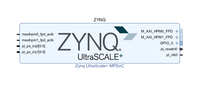
Click on the thick "+" sign in the "Diagram" window, and in the "Search" window that pops up type "ZYNQ". That will bring up 2 possibilities: choose "MPSoC". This is the ARM chip (the PS, processing system). The other one that has "RF Data Converter" in the title is for what it describes. Double click on the "MPSoC" entry. It will show you a large block in the Diagram window that says "ZYNQ" and "UltraSCALE+". In the upper part of that window click on the blue "Run Block Automation". That will bring up a window, make sure everything is selected in the left window (it should be), and hit OK. Don't change anything. That will change the ZYNQ decal to have a few more ports.
Change the name of the ZYNQ block by clicking on the "Name" text window in the "Block Properties" window to the left of the "Diagram" window. Change it to "ZYNQ" and hit return. You will see that in the ZYNQ block, the title on top of the block now shows "ZYNQ". If all went well you should see this:
Add Constraints
Next let's add the constraints file as in the last tutorial, so that the bit file is compressed and there are temperature protections for the ZYNQ chip. To do this, locate the small window that is right next to the "Diagram" window, and has a "Sources" tab. Click "Sources" and then click the $+$ symbol. That brings up a popup called "Add Sources" for telling Vivado what kind of source you want to add. Select "Add or create constraints", hit Next, and in the next window click "Create File". Call it something (I used "top" so it's the same as the project) and click Finish. That will create a new file called "top.xdc". Then open "Constraints" in the "Sources" window and navigate to the file, it should be called "top.xdc". Double click and add these lines:
# compress the bitstream to make it smaller
set_property BITSTREAM.GENERAL.COMPRESS TRUE [current_design]
# enable the over-temperature shutdown features
set_property BITSTREAM.CONFIG.OVERTEMPSHUTDOWN ENABLE [current_design]
Then save the file (control-s or click the disk icon in that window banner) and you should be good to go with these constraints.
Add DMA block
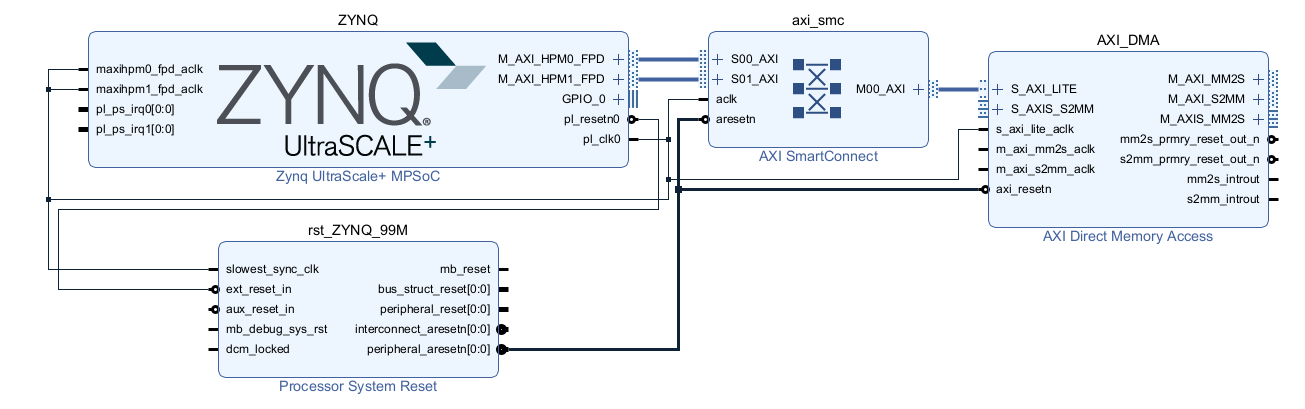
Now go back to the "Diagram" window by clicking on "Diagram" (should be on the left of the "DMA.xdc" tab). Next add the AXI DMA (explained below) by clicking on the $+$ icon in the Diagram menu bar (or right click in the diagram window and select "Add IP") and in the search window type "AXI DMA". That will bring up a list, so double click on "AXI Direct Memory Access". It will show an "AXI Direct Memory Access" decal. Click once on it and rename it to "AXI_DMA" in the "Block Properties" window. Click on the "Run Connection Automation" link, make sure everything is selected in the "Run Connection Automation" popup, and hit OK. You might have another "Run Connection Automation" link again, just click it again, make sure everything is selected in the popup, and hit OK again. Then hit the "Regenerate Layout" button (the icon is a clockwise circular arrow). You should see something like this in the diagram window:
Before going further, we should get a bit into the AXI bus, what it does, how it's used on the 4x2 board, etc.
AXI stands for "Advanced eXtensible Interface". This is a high-performance bus protocol that tries to be efficient for connecting the different parts of a "system-on-chip" (SoC). For how AXI works, see this PDF file from ARM (who define the AXI protocol). For how AMD uses AXI, see the AMD AXI Reference Guide (UG1037).
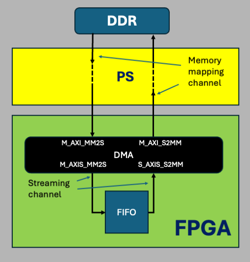
The AXI bus is pretty flexible. You can use it as a "memory-mapped" bus, which means you target addressable locations, and data is provided. Or you can also use it as a "streaming" bus, which means just send data as fast as you can, no addressing necessary. This flexibility is what allows people to design and build boards like the RealDigital 4x2 or the AMD ZCU208, that has the ZYNQ chip integrated with large amounts of fast memory. To understand how to use AXI, we need to first understand the architecture of the ZYNQ chip (ZU48DR), in the context of what we are doing in ADMX: blasting data into and out of the RF converter through FIFOs. This is described in the following diagram:
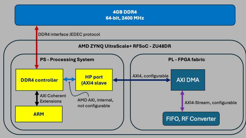
In the diagram, we see the DDR4 memory on top, consisting of 4 GBytes of 64-bit 2400MHz DDR4. The "2400MHz" refers to the data rate, and since this is double data rate (DDR), it clocks data on both edges of the clock, so for 2400 the clock will be at 1200MHz. It also refers to the maximum rate that it can be clocked, and that is the rate the ZYNQ chip uses on this board. The data width is 64 bits. This is a very complicated bus that to really understand gets you into the weeds of how DDR works, and not necessary for our purposes.
The connection between the DDR4 and the PS is through a hard silicon DDR4 controller. This gadget acts as the boundary between the AXI side of life (memory-mapped transactions) and the DDR4 memory itself (which speaks the JEDEC DDR4 protocol, not AXI). The DDR4 controller also talks to the ARM chip over an AXI-like bus (AXI Coherency Extensions) that doesn't really concern us, it's what AMD takes care of and is not relevant to the RFSoC functionality.
Between the DDR4 controller and the FPGA sits the HP port, where HP stands for "high performance". There are actually around 9 slave ports, with various properties and capabilities having to do with worrying about whether the memory in the DDR is "stale" due to caching in the CPU. But we won't have to worry about that here, because PYNQ takes care of the necessary cache flushing. So when we use PYNQ and run Python in a Jupyter notebook, we can just use the plain HP ports (not the fancier cache-coherent HPC, ACP, or ACE ports), and there are 4 of those in the PS. (The PS also presents master ports going the other direction, the HPM ports, which carry the AXI-Lite control and GPIO traffic from the CPU into the PL. These are not shown on the diagram but discussed below.)
In the PL we have an AXI DMA controller, which is the interface connection to the PS through the HP port. This is all programmable now, and you have to instantiate these blocks in your FPGA project using Vivado, which pretty much takes care of making it work. The bus between the PS HP port and the AXI DMA is pure AXI4, programmable, described below. On the other side of the AXI DMA controller is the RF Converter, and usually with a FIFO in between. The RF Converter is a real consumer (for DAC output) and producer (for ADC input) of data, and operates in a continuous way. So the AXI protocol that interfaces with these gadgets is AXI4-Stream, a pure streaming protocol that just blasts data continuously without any addressing.
So to get data into and out of the FPGA we use the AXI4 mode, which is a memory mapped scheme that allows bursting. On the RF Converter (and FIFO) side, we use a pure AXI4-Stream mode. Actually, there is another slower and simpler memory-mapped AXI4 bus called AXI4-Lite, which is a single transfer memory mapped (addressing) bus with no bursting. This is used for controls, and for GPIO. Vivado handles the connections for the AXI4-Lite ports so that you don't have to worry about it.
Note that the way AXI4 is set up, and the way the ZYNQ chip is designed, the data path into and out of the FPGA is always initiated by the FPGA, which means that the AXI DMA blocks are AXI4 masters and the HP port is always an AXI4 slave, and the DDR4 memory is a slave device accessed by the FPGA. So to blast data into the FPGA, you have to tell the AXI DMA engine inside the FPGA to start asking for data, and you tell it this using the AXI4-Lite bus via control commands. The control path is the reverse: those AXI4-Lite commands are initiated by the CPU (the master), reaching into the PL through an HPM port to poke the DMA's registers.
AXI4 is a high speed protocol that allows "bursting". In AXI, a burst consists of some number of "beats", and each "beat" consists of a vector of data which can have a width of 8, 16, 32... up to 1024 bits (yes, 1024 means there are 1024 separate physical wires!). For writes, there is also a strobe signal for each byte lane (called WSTRB, so 32 strobes on a 256-bit bus, or 128 on a 1024-bit bus) that marks which bytes in a beat are actually written. This is how AXI supports partial, unaligned, and narrow writes on a wide bus — it is a byte-enable mask, not error protection. Reads have no strobe: the full width comes back and the master simply uses the bytes it asked for. But each bit is clocked on the same rising edge of the same clock, which means that a lot of care has been taken to make sure the boards are carefully laid out to make the data paths uniform, and that inside the FPGA, the routing is done carefully so that all bits satisfy the same timing constraints.
In AXI4 there are 5 independent "channels":
| Channel | Function | Purpose |
|---|---|---|
| AW(write address) | Master $\to$ Slave write transactions with address | Send starting address, burst length, size, once per write burst |
| W:(write data) | Master $\to$ Slave, write transactions, data | These are the actual data beats |
| B:(write response) | Slave $\to$ Master, write response | Write acknowledge, completed ok (or not), once per burst |
| AR:(read address) | Master $\to$ slave read transactions, address | Send starting address, burst length, size, once per read burst |
| R:(read data) | Slave $\to$ Master read transactions, data | Data beats coming back (plus response code on each beat) |
Every channel has a "handshaking" using the VALID and READY lines, and the rule is the same on all five: the source of the channel asserts VALID when it has something to send, the destination asserts READY when it can accept it, and the transfer happens on the clock edge where both are high. What differs between channels is only who is the source. On the AW, W, and AR channels the master is the source (so the master drives VALID, the slave drives READY). On the B and R channels the slave is the source (so on the read-data channel it is the slave that asserts VALID and the master that asserts READY, the reverse of a write). One rule to keep straight: a source must not wait for READY before asserting VALID, but a destination is allowed to wait for VALID before asserting READY. This VALID/READY handshake is also what provides the backpressure that keeps the RF Converter from starving or overflowing.
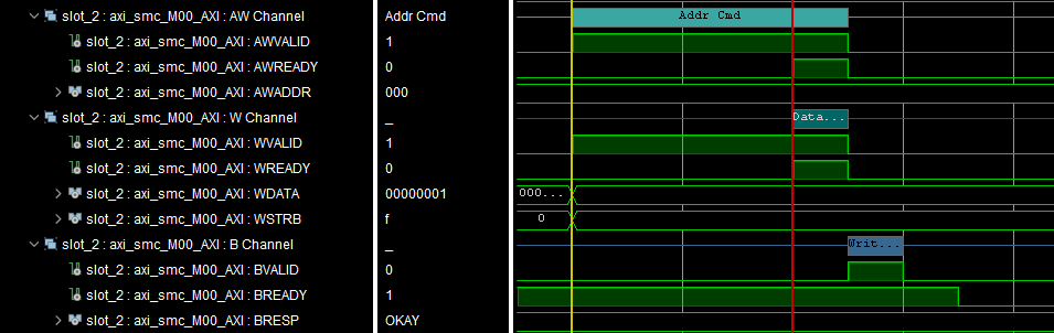
As an example, the figure below shows a transaction where the master is writing to a control register somewhere. You can see that AWVALID and WVALID both go high at the same time indicating that the address (here 0x0) and data (here 0x1) are ready. Then the slave asserts AWREADY indicating that it is latching the address, and WREADY indicating it is latching the data, on that clock edge when both valid and ready are high. But there is more to do - the slave has to determine if the transfer is complete, and if the data it received is legitimate, especially the address. So to do this, the master must also at some point (and this is usually early in the write operation) assert the ready line BREADY in the B channel when it is ready to receive the acknowledgement from the slave that the data is processed, in which case the slave asserts BVALID indicating that the operation is complete. Thus there are several handshakings going on, in each channel AW, W, and B. All handshaking follows the rule that the handshake happens on the positive edge of the clock when both valid and ready are high. Note that for the B channel, when the slave asserts BVALID it also asserts BRESP, which is a 2-bit word that tells if the operation is successful: 00=okay, 01=exclusive access ok, 10=slave error (bad address, permission denied, etc), and 11=decode error (address doesn't exist). In the figure below, BRESP is indeed 00, which is the normal response code.
In this project, we will create a buffer in the 4GBytes of DDR memory on the board that is connected to the processor. The DMA reads that buffer out of DDR over AXI4 (memory-mapped) and streams it over AXI4-Stream into a FIFO. Then we can stream back out of the FIFO and have the DMA write it into another buffer, also in DDR. So it will be important to understand the difference between the AXI ports that connect the FPGA to the processor (which is connected to the external DDR), and the AXI ports that stream that data into and out of FIFOs (or RF converters, etc. for the future).
The basic idea is that we will use all 3 kinds of AXI (AXI4-Lite, AXI4, and AXI4-Stream). AXI4-Lite connects the ARM processor in the PS to all the AXI slaves (the DMA engine, and any GPIO blocks you might have — in this project we will have a few); this is the control path, and the CPU is the master on it. The full AXI4 (memory-mapped, bursting) path runs between the AXI DMA in the PL and the PS memory, through the HP port. Here the DMA is the master: it reaches back into DDR and pulls the data itself (for transmit) or pushes captured data out to DDR (for receive). The CPU is not in this data path. The AXI4-Stream path is where the AXI DMA engine streams data into and out of the AXI FIFO. The DMA engine does a lot of heavy lifting, as it is the interface between the PS and the PL, and more specifically, the bridge between the memory-mapped world (AXI4 to DDR) and the streaming world (AXI4-Stream to the FIFO/converter).
The figure below is a schematic of the DMA ports that connect to the PS/DDR side and to the
stream (here a FIFO) side
for this project.
We use a FIFO here that understands the AXI protocol, but when you build a project that
uses the RF Converter, data will be streamed into and out of the converter through these
FIFOs. Here we will only use 1 FIFO and stream into and out of it via the AXI DMA
engine. Note the four data ports on the DMA: on the memory-mapped side, both
M_AXI_MM2S (read from DDR) and M_AXI_S2MM (write to DDR) are AXI4
masters, because the DMA initiates every DDR access; on the stream side,
M_AXIS_MM2S drives the FIFO and S_AXIS_S2MM receives from it. (The
DMA also has an S_AXI_LITE control port, the AXI4-Lite slave described in the
previous section, which is not drawn in the figure below.)
Configure DMA block
Now that we've configured our project to use block design and instantiated the PS (ZYNQ chip) and the DMA engine, now we want to configure the DMA and connect it to the PS. So double click the AXI_DMA block and open up the "Re-customize IP" settings window. You should see this:
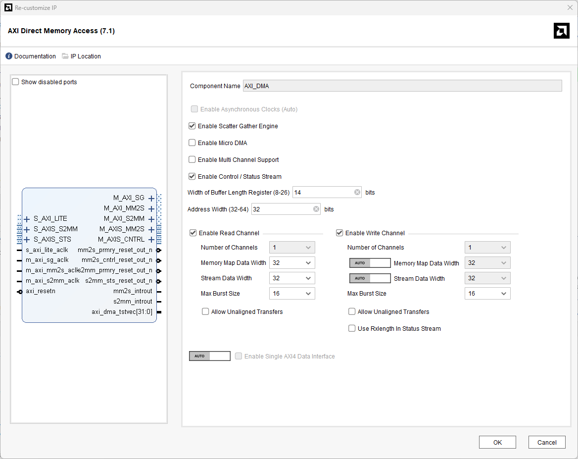
Uncheck "enable Scatter Gather Engine" for this tutorial, and set the "Width of Buffer Length Register (8-26)" to 26 if it's not there already. This sets the maximum package size for a single DMA transfer, 26 bits, which is 67 Mbytes (you can set it smaller value but it apparently saves only a small amount of memory in the FPGA). Also keep the "Address Width (32-64)" to 32, but you can also use 64 since the 4x2 uses the ZYNQ Ultrascale+, which has a 64 bit processor, however most of the time we won't be transfering enough data to worry about 64 bit addressing.
Then make sure that the DMA read and write channels are enabled, and leave the write channel set to "Auto". The "Stream Data Width" should be 32 for this tutorial. And make sure "Allow Unaligned Transfers" is not enabled so that all transfers align on the 1st byte of each 32 bit word. Click OK to accept changes.
Note that what's connected to the AXI_DMA here is only the S_AXI_LITE port, which is for controls. None of the other AXI ports on AXI_DMA (M_AXI_MM2S, M_AXI_S2MM, M_AXIS_MM2S, S_AXIS_S2MM) are connected.
Before we connect all the AXI_DMA ports, let's first take a look at the AXI_DMA block that you created. At the top right you will see "M_AXI_MM2S", "M_AXI_S2MM", and "M_AXIS_MM2S", and at the top left you will see "S_AXI_LITE" and "S_AXIS_S2MM". The first letter "M" means "master" (the DMA engine initiates transfers and produces data) and the first letter "S" means slave (the DMA engine accepts data). These ports are:
Back in the diagram, if you mouse over the $+$ sign next to the "M_AXI_MM2S" port on the AXI block, you will see the cursor change to a double chevron symbol:
If you click on that $+$ symbol that the chevron points to it will open up all of the lines on that "MM2S" port, and you will see all of the channels there. For instance you will see a "m_axi_mm2s_arready" port, which is the ready line for the AR channel. And so on. These MM2S and SS2M ports will have to be connected to the ZYNQ chip.
Next we want to connect those AXI_DMA DMA ports. The control port, "S_AXI_LITE", is already connected (it was connected when you hit the "Run Connection Automation" button after setting up the AXI_DMA block).
Configure ZYNQ block for DMA
The master ports "M_AXI_MM2S" and "M_AXI_S2MM" ports go through the processor. The ports on the ZYNQ processor are not connected by default, so we have to connect them by hand. To do this, double click the ZYNQ block, which should bring up the settings menu:
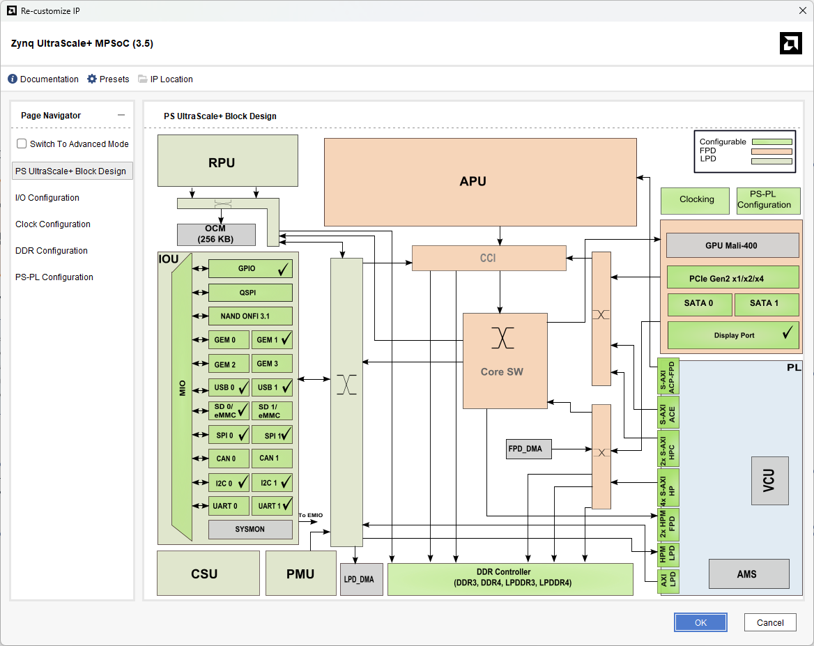
Click on the "PS-PL Configuration" tab on the left (PS is the processor and PL is the FPGA logic). then expand "PS-PL Interfaces" and then "Slave Interface". You will see 3 submenus: "AXI HP", "S AXI ACP", and "S AXI ACE". These are different PS-PL (processor-FPGA) interfaces on the ZYNQ chip, meaning that they are ports where the PL acts as a master and the PS acts as a slave.
Click "Run Connection Automation" again, enable "All Automation" in the window that pops up, and click ok. If you get a warning message, click OK to accept it and then click "Run Connection Automation" again and that should fix it. If you don't get a warning message, then click "Run Connection Automation" again if it's available. Since the S_AXI_HP0_FPD port is for DMA, it will be automatically routed to the AXI_DMA ports.
Click "Regenerate Layout" again, and you should see this:
Notice now that the M_AXI_MM2S and M_AXI_S2MM ports are routed through an "AXI SmartConnect" to the processor slave port S_AXI_HP0_FPD, which are how the processor talks to the external DRAM. And since we are only using this one port on the ZYNQ, it means that we are using the same port for reading from DDR into the FPGA and writing to the DDR from the FPGA. This port is capable of sustaining several GB/s bandwidth to DDR, and we will likely never be reading and writing at the same time, which is why one port suffices. If we want, we could enable a second port on the ZYNQ, for instance S_AXI_HP1_FPD, but our workload is not so demanding here that we need it.
The SmartConnects are there to do housekeeping things like matching different data widths, handle different clock domains, ensure correct protocol translation, and other essential housekeeping. It acts as a central AXI bus router. The system also added a "Processor System Reset" block to generate properly synchronized reset signals for the various clocks and logic, and this is especially important with designs that have various clocks.
Add a AXI FIFO
Next we want to connect the AXI stream ports, which means where we want to send the data that comes out of the external DRAM. In this tutorial, we will add a FIFO to the data path (just to see how it's done) and then loop it back. To do this, click the $+$ sign (or right click and select "Add IP") and in the window that pops up, search for "FIFO". You should see 5 or 6 variations. The one you want is "AXI4-Stream Data FIFO". This is the simplest and most lightweight of the choices you will see (e.g. "AXI-Stream FIFO" is for low throughput control data, etc, and "AXI Data FIFO" is a more complicated FIFO that is a memory mapped to memory mapped buffer and not really good for streaming).
Double click on "AXI4-Stream Data FIFO" and you should see a new block that has a title "axis_data_FIFO_0" (or something like that) appear somewhere in the "Diagram" window. Click on the block and in the "Block Properties" window that shows up (just to the left of the diagram) change the "Name:" field to "AXI_FIFO", just to make things easier when using the python hooks.
To configure the FIFO, double click on the "AXI_FIFO" block, and a "Re-customize IP" window should pop up. Under the "General" tab, set the "FIFO depth" to 512, and make sure that "TDATA width (bytes)" is set to 4 (32 bits) by first clicking on the "AUTO" button, and it will change to "MANUAL". Leave everything else as default. Then click on the "Flags" tab. Under "Write flags" change "Enable write data count" to Yes, and do the same under "Read flags" and set "Enable read data count" to Yes. This way we can find out in python how much data is in the FIFO. Click OK, and it will then show a FIFO block that has 2 more ports under "M_AXIS": "axis_wr_data_count[31:0]" and "axis_rd_data_count[31:0]". Note that the write data count will count the number of words written, and the read data count will count the number of words that are available to be read. So the number read will be the difference between these two counters (not sure exactly why they do it this way instead of counting the number actually read out).
Add AXI GPIO blocks
Next, add 3 "AXI GPIO" blocks. Two will be for the FIFO read and write data count, and the 3rd so that we can add a version number that can be read out. This is a common practice: anytime you make a change to some firmware you can change the version number so that you can know for sure what firmware is loaded. Rename 2 of them to "FIFO_WR" and "FIFO_RD", and the 3rd to "VERSION". Mouse over the + sign next to any of the GPIO ports and open up the port. You will see a port called "gpio_io_i[31:0]" with an arrow indicating it's an input. (There is also a gpio_io_o and a gpio_io_t for tristate but we don't need them here since we are only using the GPIO to read the values from the FIFO.) Now let's connect the FIFO read and write counts to the GPIO input ports so you can read them out. This has to be done by hand, but it's pretty easy in Vivado: mouse over the port you want to connect, and the cursor will change to a slanted pen. Then click and drag to the destination port and release. The system will route the line so that it looks as uncomplicated as possible. So with the Vivado pen, connect the FIFO_WR gpio_io input port to the axis_wr_data_count port on the FIFO, and do the same for the FIFO_RD.
For the version, add a "CONSTANT" block and double click on it. Change the "Const Width" to 32, and the "Const Val" to whatever you want the version to be. Let's change it to 0xa5000001 so that when we read it out, and print in hex, we will see the a5 as the confirmation it's the right value and the bottom bits can be the version (here it would be version 1). Click "OK" in the constants window, then connect the constants output to the input of the VERSION GPIO block.
Connect DMA to AXI FIFO
Next make the following connections to connect the AXI_FIFO ports to the DMA ports. You do this by mousing over the port you want to start with, and the cursor changes to a pen, then click and drag to the connecting port and release. (Sometimes it gets finicky and won't connect correctly, so try zooming in to make it easier for the system to know what you are pointing at.)
Then click on "Run Connection Automation" and enable everything in the "Run Connection Automation" window, hit OK, and then "Regenerate Layout". That should take care of connecting the AXI GPIO blocks FIFO_WR and FIFO_RD AXI bus ports, clocks, and resets. If all goes well you should see something like this:
Press F6 to run design validation (checks for errors) and make sure there are no errors, which there shouldn't be. Then go to the "Sources" tab (upper window to the left of the diagram), open "Design Sources", and right click on "DMA (DMA.bd)" and select "Create HDL Wrapper" and choose "Let Vivado manage wrapper and auto-update" and hit OK. You should then see "DMA_Wrapper (DMA_wrapper.v) (1)" in the sources window under "Design Sources". Assuming all goes well, generate the bitstream and hwh file by clicking "Generate Bitstream" in the Project Manager window on the left.
Using PYNQ
Next, make sure the board is on and connected to a PC, and open up a Jupyter lab connection in a browser (Chrome works fine). You will need to copy the .bit and .hwh files from the above project onto the board first. The .bit file is in the project subdirectory DMA.runs/impl_1/ and is named DMA_wrapper.bit and .hwh is in the project subdirectory DMA.gen/sources_1/bd/DMA/hw_handoff/ and is named DMA.hwh. Rename DMA_wrapper.bit to DMA.bit in the Jupyter notebook so that DMA.bit and DMA.hwh have the same filename.
Open up a new notebook and in the first cell type:
    from pynq import Overlay, allocate
    from rfsoc4x2 import oled
    from pynq.lib import AxiGPIO
    import numpy as np
This will load in all the libraries you need. The "oled" library from rfsoc4x2 is so you can write
to the OLED display.
In the next cell we will load the bit file (we called it "DMA.bit") into the FPGA:
    base = Overlay("DMA.bit")
    print("overlay completed")
The call to the Overlay() function actually loads the bit file into the FPGA, but it also parses the
hwh file, which is a rather large XML file will all of the information that PYNQ needs to interface the
processor with the logic (PS to PL).
You should look at the dictionary to be sure you have everything under control, so in the next cell type:
base.ip_dict
You should see 5 entries: "ZYNQ" for the processor, and "AXI_DMA" for the AXI DMA block,
and the 3 AXI GPIO blocks ("VERSION", "FIFO_RD", and "FIFO_WR"). It should
look something like this:
    ↓ip_dict:
      →AXI_DMA:
      →FIFO_RD:
      →FIFO_WR:
      →VERSION:
      →ZYNQ:
Expand AXI_DMA and you can see what's in there. The physical address assigned to the IP block starts at "phys_addr", and this is where the block is mapped into the processor's address space. "addr_range" tells you how many bytes of address space the IP block occupies. All of these addresses from phys_addr:phys_addr+addr_range are accessible via the MMIO function in PYNQ. For more on these addresses, see the documentation, which you can get by searching the web for "AXI DMA v7.1 IP product guide" (we are using v7.1 IP here), or going directly to:
on page 70 for "Simple DMA" (that is, not Scatter-Gather). This document is hard to read, so here's a synopsis.
AXI DMA Register Address Mapping
The AXI DMA has 2 memory mapping channels: MM2S from external DDR through the PS into a stream; and S2MM from stream to external DDR memory. Each has a control register at address offset 0x0 for MM2S and 0x30 for S2MM, and a status register at address offset 0x4 for MM2S and 0x34 for S2MM. You can see these by opening up the →registers: option inside AXI_DMA, and open up →MM2S_DMACR: (MM2S DMA control register) and →S2MM_DMACR: and then then →fields option on both. The control register bits look like this:
Bits are under →fields: and are described here:
Bits are described here:
The control register is written to (controlled by) the PS via the PYNQ functions you call, and the status register tells you what state things are in. For what we are doing, which is very simple DMA, the main bit for the control register is bit 0, the RS bit, where RS=0 means the DMA is stopped and RS=1 means it is running. The status register bits that we most care about are bits 0 and 1. Bit 0 is the HALT bit, so HALT=0 means the DMA channel is "RUNNING", and HALT=1 means it is "HALTED". Bit 1 is the IDLE bit, and IDLE=0 means not idle and IDLE=1 means the channel is IDLE. There are also some error bits in the status register. PYNQ takes care of these bits, you don't have to write to them explicitly!
Back to PYNQ and Python. Next let's read out the version number via AXI GPIO and place the number in the OLED display on the board. To do this, first define the mask needed for GPIO, the objects to read out the VERSION number. Then read the version, print it, and place it in the OLED display:
    mask = 0xFFFFFFFF
    version_ip = base.ip_dict["VERSION"]   # "VERSION" matches what is printed by base.ip_dict
    version_ptr = AxiGPIO(version_ip).channel1
    version = version_ptr.read()
    print(f"Firmware version: 0x{version:08x}")
    oled_display = oled.oled_display()
    oled_display.write(hex(version)+"\nLoaded!!!")
That should result in the version "0xa5000001" typed out and 2 lines of "0xa5000001" and "Loaded!!!"
onto the OLED.
Next we set up the object that allows you to do DMA:
dma = base.AXI_DMA
where AXI_DMA is the name you gave the DMA engine in the block diagram (and which should
be what the base.ip_dict command reports). When you issue this command, PYNQ will set up
the DMA engine, writing to the MM2S and S2MM control registers. To see the state of
those registers, the easiest thing to do is to write after the above command the
following:
dma.register_map
This will print out a list of registers that looks like this:
RegisterMap {
  MM2S_DMACR = Register(RS=1, Reset=0, Keyhole=0, Cyclic_BD_Enable=0, IOC_IrqEn=0, Dly_IrqEn=0, Err_IrqEn=0, IRQThreshold=1, IRQDelay=0),
  MM2S_DMASR = Register(Halted=0, Idle=0, SGIncld=0, DMAIntErr=0, DMASlvErr=0, DMADecErr=0, SGIntErr=0, SGSlvErr=0, SGDecErr=0, IOC_Irq=0, Dly_Irq=0, Err_Irq=0, IRQThresholdSts=0, IRQDelaySts=0),
  MM2S_CURDESC = Register(Current_Descriptor_Pointer=0),
  MM2S_CURDESC_MSB = Register(Current_Descriptor_Pointer=0),
  MM2S_TAILDESC = Register(Tail_Descriptor_Pointer=0),
  MM2S_TAILDESC_MSB = Register(Tail_Descriptor_Pointer=0),
  MM2S_SA = Register(Source_Address=0),
  MM2S_SA_MSB = Register(Source_Address=0),
  MM2S_LENGTH = Register(Length=0),
  SG_CTL = Register(SG_CACHE=0, SG_USER=0),
  S2MM_DMACR = Register(RS=1, Reset=0, Keyhole=0, Cyclic_BD_Enable=0, IOC_IrqEn=0, Dly_IrqEn=0, Err_IrqEn=0, IRQThreshold=1, IRQDelay=0),
  S2MM_DMASR = Register(Halted=0, Idle=0, SGIncld=0, DMAIntErr=0, DMASlvErr=0, DMADecErr=0, SGIntErr=0, SGSlvErr=0, SGDecErr=0, IOC_Irq=0, Dly_Irq=0, Err_Irq=0, IRQThresholdSts=0, IRQDelaySts=0),
  S2MM_CURDESC = Register(Current_Descriptor_Pointer=0),
  S2MM_CURDESC_MSB = Register(Current_Descriptor_Pointer=0),
  S2MM_TAILDESC = Register(Tail_Descriptor_Pointer=0),
  S2MM_TAILDESC_MSB = Register(Tail_Descriptor_Pointer=0),
  S2MM_DA = Register(Destination_Address=0),
  S2MM_DA_MSB = Register(Destination_Address=0),
  S2MM_LENGTH = Register(Length=0)
}
In the above, "DMACR" means DMA control register, "DMASR" means status register, and there are a bunch more
registers that have to do with DMA pointers that we don't have to care about because PYNQ knows what it is
doing. Focusing on the control and status registers, you will see this:
RegisterMap {
  MM2S_DMACR = Register(RS=1, Reset=0, Keyhole=0, Cyclic_BD_Enable=0, IOC_IrqEn=0, Dly_IrqEn=0, Err_IrqEn=0, IRQThreshold=1, IRQDelay=0),
  MM2S_DMASR = Register(Halted=0, Idle=0, SGIncld=0, DMAIntErr=0, DMASlvErr=0, DMADecErr=0, SGIntErr=0, SGSlvErr=0, SGDecErr=0, IOC_Irq=0, Dly_Irq=0, Err_Irq=0, IRQThresholdSts=0, IRQDelaySts=0),

  S2MM_DMACR = Register(RS=1, Reset=0, Keyhole=0, Cyclic_BD_Enable=0, IOC_IrqEn=0, Dly_IrqEn=0, Err_IrqEn=0, IRQThreshold=1, IRQDelay=0),
  S2MM_DMASR = Register(Halted=0, Idle=0, SGIncld=0, DMAIntErr=0, DMASlvErr=0, DMADecErr=0, SGIntErr=0, SGSlvErr=0, SGDecErr=0, IOC_Irq=0, Dly_Irq=0, Err_Irq=0, IRQThresholdSts=0, IRQDelaySts=0),
}
So you see that the MM2S and S2MM control registers both have RS=1 set, so it is in the "RUN" state.
That's because it is waiting for you to initiate the DMA transfer. The status registers both have
HALT=0 and IDLE=0 which means the channel is running and not IDLE, consistent with what
the control register is telling it. Also remember, MM2S means "memory-map to stream" and describes
reading from external DDR and send it to the FPGA. S2MM means "stream to memory-map" and describes
the opposite: reading from the DMA stream (here it's a FIFO) and writing it to DDR.
A little bit on how the RealDigital 4x2 memory works. There is 4GByte for the processor system (PS) and another 4GByte for the programmable logic (PL). It is all 2400MHz DDR. The 4G PS memory is used by the Linux kernel, PYNQ applications, general system use, and buffers allocated in notebooks (see below). Once you boot up the board, you can check how the system is using DDR memory and especially how much contiguous memory is free by looking in the Linux file /proc/meminfo. To do this in a notebook, try this:
!cat /proc/meminfo | grep -E "MemTotal|MemFree|Cached|Active|Inactive|Cma"
On the board I'm using (v3.1.1), here's what I see:
MemTotal:        4023308 kB
MemFree:         3022924 kB
Cached:           395848 kB
SwapCached:            0 kB
Active:           223096 kB
Inactive:         671476 kB
Active(anon):       1788 kB
Inactive(anon):   455584 kB
Active(file):     221388 kB
Inactive(file):   215892 kB
CmaTotal:         131072 kB
CmaFree:          124968 kB
MemTotal is around 4G, and this is the PS external DDR memory that you have access to via PYNQ. The 4G PL memory is not visible to Linux by default, but can be manually configured and accessed in the Xilinx project (using the AXI MIG interface, which is not covered here). The numbers above will change all the time, but the ones you really care about are the last 2: CmaTotal and CmaFree. CmaTotal has to do with how you boot up the machine, and can be changed. Since there's 4G (MemTotal is around 4G) then it's a little wasteful to only have 131MB contiguous memory available since there's 3G free here (MemFree). We will get to that later.
Next, allocate buffers in the external DDR. We want a buffer that we can initialize with some values, and send to the AXI FIFO, and another buffer that we can write into from the FIFO and verify that it has the right data. We will use the PYNQ allocate() function from the pynq.allocate module, which will allocate in the external DRAM DDR memory, not in the processor internal memory. We will use numpy to specify what type of memory (uint32 here). Note that allocate() requires memory that is physically contiguous (no gaps), is shared between the processor and FPGA, and will be reserved so that Linux won't touch it. Below we allocate 2 buffers: into_buffer is the buffer we will allocate and fill with data to write into the FIFO, and from_buffer is the buffer that will receive data from the FIFO to compare. Note that we make these buffers the same size, mostly for convenience but also because that makes the DMA go smoothly without any need for us to do anything. Both buffers are 32 bit unsigned integers. After allocating the buffer, we will write a counter into the input buffer that will be sent to the FIFO, but let's also set the upper 16 bits of the counter to something we can easily recognize.
    into_size = 100
    into_buffer = allocate(shape=(into_size,), dtype=np.uint32)
    for i in range(into_size):
        into_buffer[i] = 0xcafe0000 + i
        print(hex(into_buffer[i]), end=" ")
    from_size = 100
    from_buffer = allocate(shape=(from_size,), dtype=np.uint32)
This should print out all 100 elements of the into_buffer so you can see if it's ok.
Now we have to set up the pointers for the dma channels for both sending and receiving:
    dma_send = dma.sendchannel
    dma_recv = dma.recvchannel
Next we set up the AXI GPIO objects so we can read the data count from the FIFO.
The FIFO_WR GPIO will contain the number of words written to the FIFO, and the
FIFO_RD GPIO block will contain the number of words that can be read from the FIFO
at any given time. Here is the code to create the objects:
    FIFO_rd_ip = base.ip_dict["FIFO_RD"]
    FIFO_rd_ptr = AxiGPIO(FIFO_rd_ip).channel1
    FIFO_wr_ip = base.ip_dict["FIFO_WR"]
    FIFO_wr_ptr = AxiGPIO(FIFO_wr_ip).channel1
Next we initiate the DMA transfer. Note that when writing to and reading from a FIFO, it's always best to initiate the read first, and then the write. This is because if the write goes first, and you write more than what the FIFO can hold, you will lose data (when the FIFO is full, it won't accept more data). Then when you read you won't get everything, data will be lost. But if you initiate the read first, then of course when it starts the FIFO is empty so it waits for data. Then when the write starts, the FIFO starts filling up, is no longer empty, and so the read keeps reading and if you send more data than the FIFO can hold, it's ok because the reading and writing will happen at the same clock speeds, and you won't miss anything. However, here we have a simple FIFO that has more space than the buffers we are going to send. So just to illustrate the FIFO read and write counts, we are going to do things in order: send the into_buffer, wait for the transaction to finish, read the FIFO write count and the FIFO read count. Then fill the from_buffer from the FIFO, wait for completion, then read the FIFO read count.
The transfer is simple, just use the transfer method for the dma_send and dma_recv objects, for example dma_send.transfer(into_buffer). However there are more arguments to that method that tells you where to start in the buffer and how many words to send. So the command dma_send.transfer(into_buffer) is equivalent to dma_send.transfer(into_buffer, 0, 4*into_size), since the default is to start at 0 and read everything.
Note that the wait() method is blocking, so no code is executed until the dma transfer is finished.
    dma_send.transfer(into_buffer)
    dma_send.wait()
    FIFO_wr_data = FIFO_wr_ptr.read()
    FIFO_rd_data = FIFO_rd_ptr.read()
    print("Fifo words written : "+str(FIFO_wr_data))
    print("Fifo available to read: "+str(FIFO_rd_data))
    dma_recv.transfer(from_buffer)
    dma_recv.wait()
    FIFO_rd_data = FIFO_rd_ptr.read()
    print("Fifo words available after transfer "+str(FIFO_rd_data))
If after all that
you were to read the control and status registers now by putting a "dma.register_map" after
the "dma_recv.wait()" command, you should see the MM2S is still in "RUN" state (RS=1),
and the status register will report it is "RUNNING" (HALT=0) and "IDLE" (IDLE=1)
because the transfer is complete.
At this point the data in the from_buffer should be the same as the data in the into_buffer, and you can check that by printing it out.