We will build on the previous XADC project here, adding capability for the FPGA to latch data and then send to the RPi for display by pushing a single button. The RPi can then display the value in some form (maybe even graphical if you are ambitious enough) so that you now have a real voltmeter built from Verilog and Python. Yes, this is overkill compared to a cheap voltmeter you can buy, but it does have quite a few of the necessary pieces to make a more sophisticated data acquisition system.
Best to go through the FPGA<->FPGA-RPI Serial Communication lab so that you are up to speed on UARTs and how to get the BASYS3 to use it to talk to the RPi.
Our top level will be similar to the previous project, so we will need our top level (top.v) to have the following:
clock; reset, version, and latch push buttons with the latch debounced; adc_n and adc_p analog inputs to be digitized; rx receive line from the RPi
segment, dp, and digit outputs for the 4 7-segment displays; led outputs; tx transmit line to the RPi; JB for debugging (we probably don't need the JA as in the previous project, JB will be enough)
The top level should look like this:
module top(
    input clock,            // system clock
    input reset,            // BTNR
    input version,          // BTNU
    input latch,            // BTNL
    input adc_n, adc_p,     // VCAUX 6, P and N
    output reg [15:0] led,      // 16  onboard LEDs above the switches
    output [6:0] segment,   // 4 digit LED display
    output dp,              // "." next to each LED digit
    output [3:0] digit,     // which of the 4 digits to drive
    output [7:0] JB,        // PMOD display for debugging
    input rx,               // UART receive
    output tx               // UART transmit
    );
    parameter VERSION = 'h0001;
Note the last 2 IO lines for the UART transmit (tx) and receive (rx). Also, the last line above isa parameter that will change when we change the firmware version, set to 1 initially. We will be adding code below that will allow you to send the version to the 4 7-segment display so we can see what we have. We will make it 16 bits wide so that it will be consistent with the 16 bits of the XADC value that we will read out (this makes the readout less complicated!). Also note that the led output is a reg here, because it will be latched inside the state machine that controls transmitting the data to the RPi (see below).
The instatiation for the UART transmitter and receiver is just like in the above mentioned project, however we are going to change the clock that drives the UART from 100MHz down to 25MHz. We are doing this because we are invariably going to need to look at signals out of the BASYS3 PMOD ports for debugging using a logic analyzer (see Logic Analyzer (for Debugging)), and the one used here is a bit slower than 100MHz.
To make a 25MHz clock we just make a 2 bit counter, and use the MSB to divide the clock by 4, and put the new 25MHz clock out on a BUFG clock line:
    //
    //  make a slower clock for the UART transmitter and for the FSM
    //  below that controls it.   We do this because the logic analyzer
    //  is slow too, it will only look at 8 wires at 25MHz.   So if we
    //  divide the system clock by 4, that will give us a 25MHz clock
    //  and that should do nicelly, and it will make clocks_per_bit come
    //  out as an integer
    //
    reg [1:0] count2 = 0;
    always @ (posedge clock) count2 <= count2 + 1;
    wire clock25;
    BUFG clk25buf (.I(count2[1]), .O(clock25) );
We will also need a 104MHz clock as before, to drive the XADC so that we get samples at 1MHz. We do that by running the PI Catalog, search for "clocking wizard" in the search window, double click on "Clocking Wizard" in the list below. Change the name to clock_104 in the component window, set the "Output Clock" to 104MHz and hitting OK and Generate.
Then instantiate like this:
    //
    //  generate a 104MHz clock for the XADC so we can get samples at 1MHz
    //
    wire locked, clock104;
    clock_104 XADC_CLOCK(
        .reset(reset),
        .locked(locked),
        .clk_in1(clock),
        .clk_out1(clock104)
    );
You need to add a deboucer for the latch push button only (reset and version do not need debouncing, although it wouldn't hurt if you add them). Note that at some point below we will have to build a state machine to send data to the RPi, and that state machine will want to be in phase with the uart tx module. If we are going to use the latch debounced signal to trigger the state machine, let's drive the debouncer with the 25MHz clock. Note that the debouncer will wait 100,000 ticks, so that's 4ms given the 40ns period, but that's ok. Let's use the same debouncer as was introduced in the FPGA<->FPGA-RPI Serial Communication project, the one that has the number of ticks as input. The instantiation should be:
    //
    //  debounce the latch push button
    //
    wire latch_level, latch_pulse;
    debouncer DEBOUNCE_LATCH(
        .clock(clock25),
        .button(latch),
        .ticks(17'd25000),      // 25k x 40ns = 1ms
        .level(latch_level),
        .pulse(latch_pulse)
    );
The signals latch_pulse will be a debounced pulse 1 clock period wide, or
40ns here. We won't be using latch_level.
Let's add the code for the 7-segment LED display developed in the XADC lab:
    //
    //  next drive the 4 7-segment displays
    //
    wire [15:0] display_this;
    display4 DISPLAY (
        .clk100(clock),
        .number(display_this),
        .digit(digit),
        .segments(segment),
        .period(dp)
        );
Note that display_this will be set below.
Next instantiate the UART tx (the code can be found here) with the 25MHz clock. Since we want 1μs bit widths (1000000 baud), and the clock has a 40ns period, then we need 25 clock ticks per bit. This means that the tx_done signal that come out of uart_tx will be 40ns wide, and that will mean that our FSM below should also run at 25MHz to make sure everything stays synchronous.
    //
    //  instantiate the UART transmitter
    //
    wire tx_active, tx_done;
    wire do_transmit;
    wire [7:0] transmit_byte;
    uart_tx TRANSMITTER (
        .i_Clocks_per_Bit('d25),
        .i_Clock(clock25),
        .i_Reset(reset),
        .i_Tx_DV(do_transmit),
        .i_Tx_Byte(transmit_byte),
        .o_Tx_Active(tx_active),
        .o_Tx_Serial(tx),       // tied to FPGA tx output
        .o_Tx_Done(tx_done)
        );
Next is the XADC block. You make this by clicking on "IP Catalog" and following the same instructions as in the XADC lab, but this time let's run the XADC at 104MHz. So click on "IP Catalog", search for XADC, then double click on "XADC Wizard". Let's call it "XADC_IP" in the "Component Name" window. In the "Basic" tab unselect "reset_in" and leave the "DCLK" clock at 100MHz. In the "Alarms" tab deselect all alarms and in the "Single Channel" tab select "VAUXP6 VAUXN6". Then hit OK, "Generate" at the next pop-up, and it should create a new source in the "Sources" window called "XADC_IP". Instantiate this in your top level module like this:
    //
    //  here is the XADC block
    //
    wire [6:0] daddr_in = 7'h16;
    wire adc_ready, isbusy, adc_data_ready, eos_out, alarm;
    wire [15:0] adc_data;
    wire [4:0] channel_out;
    XADC_IP XADC_INST (
        .daddr_in(7'h16),   // specifies vcaux6 pints to digitize
        .dclk_in(clock104),    // 100MHz clock
        .den_in(adc_ready), // tied to adc_ready, tells adc to convert, tieing causes continuous conversions
        .di_in(16'h0),      // to set the data to something, not used here
        .dwe_in(1'b0),      //  set to enable writing to di_in, which we don't want to do
        .vauxp6(adc_p),     //  positive input to digitize
        .vauxn6(adc_n),     //  negative input to digitize
        .busy_out(isbusy),  // tells you the adc is busy converting
        .channel_out(channel_out[4:0]), // for using more than 1 channel, tells you which one.  not used here
        .do_out(adc_data),      // adc value from conversion
        .drdy_out(adc_data_ready),  //tells you valid data is ready to be latched
        .eoc_out(adc_ready),   //  specifies that the ADC is ready (conversion complete)
        .eos_out(eos_out),     //  specifies that conversion sequence is complete
        .alarm_out(alarm),      // OR's output of all internal alarms, not used here
        .vp_in(1'b0),           // dedicated analog input pair for differential, tied to 0 if not used
        .vn_in(1'b0)
    );
    //
    // wait for XADC to tell you something is ready to latch. note this means continuous latching
    //
    reg [15:0] r_adc_data;
    always @ (negedge isbusy) begin
        if (reset) r_adc_data <= 16'h0;
        else r_adc_data <= adc_data;
        end
     //
    //  make a ~1Hz clock so we can run the LED display slower
    //
    reg [26:0] counter;
    reg [15:0] s_adc_data;
    always @ (posedge clock) begin
        if (reset) counter <= 0;
        else counter <= counter + 1;
        end
    wire clock_1hz = counter[26];
    always @ (posedge clock_1hz) s_adc_data <= r_adc_data;
    assign display_this = version ? VERSION : s_adc_data;
As you can see, we use the negedge of isbusy signal from the "busy_out" port to tell us a new value is ready, and latch it, as we saw in the previous lab Using the FPGA ADC. Also, we want the LED display to display the ADC value except when the version button (BTNU) is pushed. So we generate a 1Hz clock and use that to latch r_adc_data into s_adc_data and send s_adc_data to the LEDs.
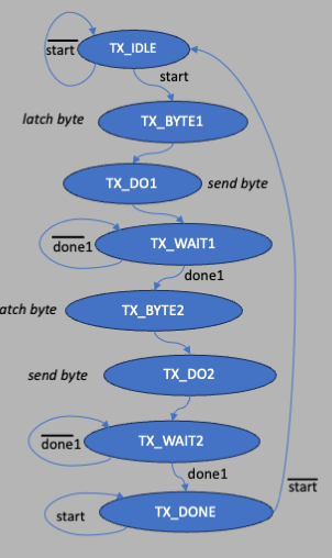
Since the adc data has 16 bits, and the UART sends 1 byte at a time (as an exercise for the student you could change the uart_tx code to send 16 bits!), we will have to have some logic that will do the following:
Here is the state machine diagram:
Also, we can latch the signal r_adc_data inside the wait state of the state machine, and when the latch button is pushed, latch that signal into the led output registers so that we can see what's being transmitted on the LEDs and compare in the RPi.
We will need 7 states. The state machine code will look like this:
    //
    //  now make a state machine to deal with transmitting 2 bytes
    //
    reg [2:0] tx_state;         // 7 states so 3 bits will do
    reg [15:0] latched_adc;     // latched adc data
    localparam [2:0] TX_WAIT=0, TX_BYTE1=1, TX_DO1=2, TX_WAIT1=3, TX_BYTE2=4,
                    TX_DO2=5, TX_WAIT2=6;
    reg doit;
    reg [7:0] tx_data;
    always @ (posedge clock25) begin
        if (reset) begin
            tx_state <= TX_WAIT;
            doit <= 0;
            tx_data <= 0;
            led <= 0;
        end
        else
            case (tx_state)
                TX_WAIT: begin
                    if (latch_pulse) tx_state <= TX_BYTE1;
                    else tx_state <= TX_WAIT;
                    doit <= 0;
                    tx_data <= 0;
                    latched_adc <= r_adc_data;
                end
                TX_BYTE1: begin
                    led <= latched_adc;                 // put this value onto the LEDs
                    tx_data <= latched_adc[7:0];
                    tx_state <= TX_DO1;
                end
                TX_DO1: begin
                    doit <= 1;
                    tx_state <= TX_WAIT1;
                end
                TX_WAIT1: begin
                    doit <= 0;
                    if (tx_done) tx_state <= TX_BYTE2;
                    else tx_state <= TX_WAIT1;
                end
                TX_BYTE2: begin
                    tx_data <= latched_adc[15:8];
                    tx_state <= TX_DO2;
                end
                TX_DO2: begin
                    doit <= 1;
                    tx_state <= TX_WAIT2;
                end
                TX_WAIT2: begin
                    doit <= 0;
                    if (tx_done) tx_state <= TX_WAIT;
                    else tx_state <= TX_WAIT2;
                end
            endcase
    end
    assign do_transmit = doit;
    assign transmit_byte = tx_data;
Let's also use the logic analyzer to look at the outputs from the JB PMOD block defined in the top.v IO. We can look at a bunch of signals:
assign JB = {clock25,tx,do_transmit,tx_active,tx_done,tx_state[2:0]};
Lastly, make a new constraints file.
## clock
set_property PACKAGE_PIN W5 [get_ports clock]
set_property IOSTANDARD LVCMOS33 [get_ports clock]

# rx is pin 4 on JC
set_property PACKAGE_PIN P18 [get_ports rx]
set_property IOSTANDARD LVCMOS33 [get_ports rx]
# tx is pin 1 on JC
set_property PACKAGE_PIN K17 [get_ports tx]
set_property IOSTANDARD LVCMOS33 [get_ports tx]

# push buttons
set_property PACKAGE_PIN T17 [get_ports reset]
set_property IOSTANDARD LVCMOS33 [get_ports reset]
set_property PACKAGE_PIN W19 [get_ports latch]
set_property IOSTANDARD LVCMOS33 [get_ports latch]
set_property PACKAGE_PIN T18 [get_ports version]
set_property IOSTANDARD LVCMOS33 [get_ports version]

# LEDs
set_property PACKAGE_PIN U16 [get_ports {led[0]}]
set_property IOSTANDARD LVCMOS33 [get_ports {led[0]}]
set_property PACKAGE_PIN E19 [get_ports {led[1]}]
set_property IOSTANDARD LVCMOS33 [get_ports {led[1]}]
set_property PACKAGE_PIN U19 [get_ports {led[2]}]
set_property IOSTANDARD LVCMOS33 [get_ports {led[2]}]
set_property PACKAGE_PIN V19 [get_ports {led[3]}]
set_property IOSTANDARD LVCMOS33 [get_ports {led[3]}]
set_property PACKAGE_PIN W18 [get_ports {led[4]}]
set_property IOSTANDARD LVCMOS33 [get_ports {led[4]}]
set_property PACKAGE_PIN U15 [get_ports {led[5]}]
set_property IOSTANDARD LVCMOS33 [get_ports {led[5]}]
set_property PACKAGE_PIN U14 [get_ports {led[6]}]
set_property IOSTANDARD LVCMOS33 [get_ports {led[6]}]
set_property PACKAGE_PIN V14 [get_ports {led[7]}]
set_property IOSTANDARD LVCMOS33 [get_ports {led[7]}]
set_property PACKAGE_PIN V13 [get_ports {led[8]}]
set_property IOSTANDARD LVCMOS33 [get_ports {led[8]}]
set_property PACKAGE_PIN V3 [get_ports {led[9]}]
set_property IOSTANDARD LVCMOS33 [get_ports {led[9]}]
set_property PACKAGE_PIN W3 [get_ports {led[10]}]
set_property IOSTANDARD LVCMOS33 [get_ports {led[10]}]
set_property PACKAGE_PIN U3 [get_ports {led[11]}]
set_property IOSTANDARD LVCMOS33 [get_ports {led[11]}]
set_property PACKAGE_PIN P3 [get_ports {led[12]}]
set_property IOSTANDARD LVCMOS33 [get_ports {led[12]}]
set_property PACKAGE_PIN N3 [get_ports {led[13]}]
set_property IOSTANDARD LVCMOS33 [get_ports {led[13]}]
set_property PACKAGE_PIN P1 [get_ports {led[14]}]
set_property IOSTANDARD LVCMOS33 [get_ports {led[14]}]
set_property PACKAGE_PIN L1 [get_ports {led[15]}]
set_property IOSTANDARD LVCMOS33 [get_ports {led[15]}]
##
## 7 segment display
set_property PACKAGE_PIN W7 [get_ports {segment[0]} ]
set_property IOSTANDARD LVCMOS33 [get_ports {segment[0]} ]
set_property PACKAGE_PIN W6 [get_ports {segment[1]} ]
set_property IOSTANDARD LVCMOS33 [get_ports {segment[1]} ]
set_property PACKAGE_PIN U8 [get_ports {segment[2]} ]
set_property IOSTANDARD LVCMOS33 [get_ports {segment[2]} ]
set_property PACKAGE_PIN V8 [get_ports {segment[3]} ]
set_property IOSTANDARD LVCMOS33 [get_ports {segment[3]} ]
set_property PACKAGE_PIN U5 [get_ports {segment[4]} ]
set_property IOSTANDARD LVCMOS33 [get_ports {segment[4]} ]
set_property PACKAGE_PIN V5 [get_ports {segment[5]} ]
set_property IOSTANDARD LVCMOS33 [get_ports {segment[5]} ]
set_property PACKAGE_PIN U7 [get_ports {segment[6]} ]
set_property IOSTANDARD LVCMOS33 [get_ports {segment[6]} ]
##
## LED period (dot)
set_property PACKAGE_PIN V7 [get_ports {dp}]
set_property IOSTANDARD LVCMOS33 [get_ports {dp}]
##
## digit select
set_property PACKAGE_PIN U2 [get_ports {digit[0]} ]
set_property IOSTANDARD LVCMOS33 [get_ports {digit[0]} ]
set_property PACKAGE_PIN U4 [get_ports {digit[1]} ]
set_property IOSTANDARD LVCMOS33 [get_ports {digit[1]} ]
set_property PACKAGE_PIN V4 [get_ports {digit[2]} ]
set_property IOSTANDARD LVCMOS33 [get_ports {digit[2]} ]
set_property PACKAGE_PIN W4 [get_ports {digit[3]} ]
set_property IOSTANDARD LVCMOS33 [get_ports {digit[3]} ]

## Buttons
set_property PACKAGE_PIN T18 [get_ports version]
set_property IOSTANDARD LVCMOS33 [get_ports version]
set_property PACKAGE_PIN W19 [get_ports latch]
set_property IOSTANDARD LVCMOS33 [get_ports latch]
set_property PACKAGE_PIN T17 [get_ports reset]
set_property IOSTANDARD LVCMOS33 [get_ports reset]

## Pmod Header JXADC
## Schematic name = XA1_P
set_property PACKAGE_PIN J3 [get_ports adc_p ]
set_property IOSTANDARD LVCMOS33 [get_ports adc_p ]
## Schematic name = XA1_N
set_property PACKAGE_PIN K3 [get_ports adc_n ]
set_property IOSTANDARD LVCMOS33 [get_ports adc_n ]

##Pmod Header JB
##Sch name = JB1
set_property PACKAGE_PIN A14 [get_ports {JB[0]}]
set_property IOSTANDARD LVCMOS33 [get_ports {JB[0]}]
##Sch name = JB2
set_property PACKAGE_PIN A16 [get_ports {JB[1]}]
set_property IOSTANDARD LVCMOS33 [get_ports {JB[1]}]
##Sch name = JB3
set_property PACKAGE_PIN B15 [get_ports {JB[2]}]
set_property IOSTANDARD LVCMOS33 [get_ports {JB[2]}]
##Sch name = JB4
set_property PACKAGE_PIN B16 [get_ports {JB[3]}]
set_property IOSTANDARD LVCMOS33 [get_ports {JB[3]}]
##Sch name = JB7
set_property PACKAGE_PIN A15 [get_ports {JB[4]}]
set_property IOSTANDARD LVCMOS33 [get_ports {JB[4]}]
##Sch name = JB8
set_property PACKAGE_PIN A17 [get_ports {JB[5]}]
set_property IOSTANDARD LVCMOS33 [get_ports {JB[5]}]
##Sch name = JB9
set_property PACKAGE_PIN C15 [get_ports {JB[6]}]
set_property IOSTANDARD LVCMOS33 [get_ports {JB[6]}]
##Sch name = JB10
set_property PACKAGE_PIN C16 [get_ports {JB[7]}]
set_property IOSTANDARD LVCMOS33 [get_ports {JB[7]}]
All should be well when you build it and load it into the
FPGA.
The above project archive can be found
here.
We now have to build a Python program on the RPi to read the data and display the voltage. This will be a variation on the tkinter program we wrote earlier, called voltmeter.py, and is displayed here:
from tkinter import *
import serial
import serial.tools.list_ports
import codecs
import time

root = Tk()


class Application(Frame):
    """ Create the window and populate with widgets """

    def __init__(self,parent):
        """ initializes the frame """
        Frame.__init__(self,parent,background="white")
        self.parent = parent
        self.grid()
        self.create_widgets()
        self.isopen = 0
        self.openPort()

    def create_widgets(self):
        self.buttonQ = Button(self, text="Quit")
        self.buttonQ["command"] = self.quitit
        self.buttonQ.grid(row=0,column=0, sticky=W)

        self.buttonR = Button(self,text="Receive: ")
        self.buttonR.grid(row=0,column=1, sticky=W)
        self.buttonR["command"] = self.getdata

        self.status = Text(self,height=1,width=30)
        self.status.grid(row=1, column=0, columnspan=2, sticky=W)
        self.status.delete("1.0",END)

    def quitit(self):
        print("That's all folks!")
        quit()

    def openPort(self):
        if self.isopen == 1:
            self.status.insert(END,"Port is already open!\n")
            self.ser.close()
            #return
        #
        #   defaults
        #
        port = "/dev/ttyS0"
        sbaud = "1000000"
        baud = int(sbaud)
        timeout = 2
        print("port="+port+"  baud="+sbaud)
        self.ser = serial.Serial(port,sbaud,timeout=timeout)
        if self.ser.isOpen():
            self.status.insert(END,self.ser.name + " is now open\n")
            print(self.ser.name + " is now open...")
            self.isopen = 1
        else:
            self.status.insert(END,self.ser.name + " is NOT open!!!\n")
            print("sorry, problem trying to open port "+port+"\n")

    def getdata(self):
        #
        # check to see if any port has been opened or not
        #
        if self.isopen == 0:
            self.status.insert(END,"Sorry but you MUST open a port first!")
            return
        #
        # now wait for input
        #
        nbytes = 2
        self.status.delete(1.0,END)
        self.status.insert(1.0,"Waiting...")
        tdata = self.ser.read(nbytes)
        ld = len(tdata)
        print(ld)
        if ld > 0:
                #
                # flag input has arrived and print out in hex
                #
                noinput = 0
                idata = int.from_bytes(tdata,byteorder="little")
                print("idata1: "+str(idata))
                val = idata/16
                print("idata: ",str(val))
                #
                #   now calculate the votage read
                #
                voltage = val * 0.244E-3
                self.status.delete(1.0,END)
                self.status.insert(1.0,hex(idata) + " = " + str(voltage)+" volts")
        else:
            self.status.insert(END,"timeout!")

def main():

    # modify the window
    root.title("Python/BASYS3 Voltmeter")
    root.wm_title("Python/BASYS3 Voltmeter")
    root.geometry("500x500+800+400")
    root.update()

    #create the frame that holds other widgets
    app = Application(root)

    #kick off event loop
    root.mainloop()


if __name__ == '__main__':
    main()
This script will show you a GUI that has a "Quit" and "Receive" button. The serial communication part is opened in the openPort function, called at the Applicationi init method, where we also set the variable isopen to 0. The openPort parameters are hard coded: port = /dev/ttyS0M, sbaud = 1000000 and converted to an integer, and timeout = 5. All the rest of the defaults are ok (8 bits, 1 start, 1 stop bit, no parity).
The way to use this is to first push the latch button on the BASYS3, that will latch a value and put it on the LEDs so you can see the 16 bits. Then, on the RPi push Receive, and you will have 2 seconds (in the python code you can see "timeout = 2") to push the transmit button on the BASYS3 board. The data will be sent to the RPi. Pushing Receive on the RPi program will call getdata. The line nbytes = 2 means we will wait for 2 bytes, and the line tdata = self.ser.read(nbytes) executes it. If it receives anything, then ser.read returns a byte string that should be 2 bytes long, so if the length is 0 then that indicates a timeout. In the getdata code it checks that the length is no 0, then converts the byte to an integer using the int.from_bytes method with byteorder="little" tells the system to convert those bytes into an integer using "little endian" ordering, which means 1st byte is the low value and 2nd byte received is the upper. The integer is then divided by 16 so that the remaining value in val will be the upper 12 bits of the returned ADC valule, and it is multiplied by the number of volts per bit which is 0.244mV as detailed here.
Note that sometimes the transfer doesn't work, and this is due to the degree to which the timing has to be right between sending and receiving.
A better thing to do would be to have the RPi send a signal to the BASYS3 saying "please send" and then have the FPGA do the transfer. (Next lab!)
Using the logic analyzer, we can look at the tx_state state machine, and the handshake between that FSM and the uart_tx module:
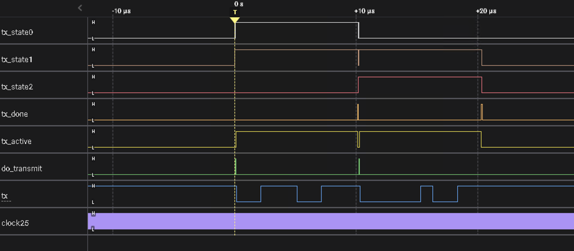
Triggerin on a positive transition of the LSB of tx_state, you can see the do_transmit signal asserted, which causes uart_tx to assert tx_active and then you see transitions in tx which means that the first byte is being sent. When the first tx_done signal is asserted, the FSM then starts sending the 2nd byte, and when tx_done is asserted a 2nd time, all is quite and the FSM goes back to the wait state, which is 0. The "clock25" signal has a solid blue but that's because it's transitioning too fast for the display to see it.
The Vivado version 2023.1 project is archived here and the RPi Python code is here.