4-Digit LED Display
The BASYS3 has a 4 digit LED display, towards the lower left corner (item 4
in the picture below)
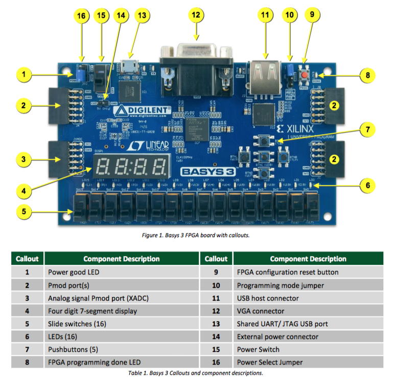
and is described starting on page 15 of the
BASYS3 manual, which states that each of the 4 digits is composed of 7
LEDs in segments arranged in a figure-8 pattern, with an additional LED for the
period in the lower right corner. So you have to have 8 outputs from your top level
verilog module, and driving the right ones can give you any particular pattern
where the most useful are the 10 decimal digits. There are also 4 signals
(see figure 16) that point to each of the 4 segments.
So the way you display a 4-digit number (or any 4-digit pattern) is to set
the patter, select the first segment, then set the pattern and select the
second, and so on, faster than the human eye can follow, which means you would
make a clock that runs at say 60Hz, and drive each one in turn. So if your
eye could see fast enough, you would not see a 4 digit pattern, but you
would instead see the 4 digits go on and off in a row.
To make a new verilog circuit to take care of all this, it would have as
inputs the system clock, and the 4-digit number you want to display.
The outputs would be connected to the outputs of top.v, which would be
segment (the 7 segments of one of the displays),
dp (the period), and digit (which digit to display). It
would look something like this:
module display4(
input clk100,
output reg [3:0] digit = 0, //digit 3 is leftmost (MSD), digit 1 is rightmost (LSD)
output reg [6:0] segments = 'b111111, //7 segments: top,mid,bot and top_left/bot_left and same for right
output reg period,
input [15:0] number //4 hex digits
);
We will use the system clock (100MHz) so that we can make a slower 60Hz clock
internal to this module. The input number will be in hex, and will be 16 bits
(4 bits per digit, 0-A). So the next thing the module will do is to separate
the 4 digits into 4 4-bit variables:
wire [3:0] digit3 = number[15:12];
wire [3:0] digit2 = number[11:8];
wire [3:0] digit1 = number[7:4];
wire [3:0] digit0 = number[3:0];
To make a clock that runs at around 60Hz (16ms period), starting with a 10ns
period, you would need a counter that has 18 bits (remember, a 1 bit counter
is a clock divider, so the period of the new clock is larger by a factor of
2N+1 for an N bit counter). So for 18 bits, the new period will
be 219×10ns = 5.2ms. That translates into 190Hz, but that's
what we want because we want to use that clock to drive each of the 4 digits,
one after the other, which means each of them turns on and off at around
47Hz, which is fine for our purposes. The code looks like this (and we
will use a BUFG to put the new clock into a clock line inside the FPGA):
reg [17:0] counter = 0;
//
// use negedge so we don't have race conditions later
//
always @ (negedge clk100) counter <= counter + 1;
wire digit_clock = counter[17];
wire clock;
BUFG clkdbuf (.I(digit_clock),.O(clock));
Note that the register we will use as the new 47Hz clock is
called clock.
Next we need a counter that tells us which digit to drive:
reg [1:0] which_digit = 0;
always @ (posedge clock) which_digit <= which_digit + 1;
Now we need some way to go from the 4-bit number in
digit1 and the other 3 digits as above, to which of
the 7 LEDs in each segment to drive. This is a tricky thing to
write, it requires you to map the 7 segments as detailed on page
16 of the manual to each digit. The code for doing this is
shown next, where the input is the 4-bit hex nmber and
the output are the 7 segments to drive:
module segnum (
input clk,
input [3:0] number,
output reg [6:0] seg = 0
);
parameter [6:0] p0 = 'b1000000;
parameter [6:0] p1 = 'b1111001;
parameter [6:0] p2 = 'b0100100;
parameter [6:0] p3 = 'b0110000;
parameter [6:0] p4 = 'b0011001;
parameter [6:0] p5 = 'b0010010;
parameter [6:0] p6 = 'b0000010;
parameter [6:0] p7 = 'b1111000;
parameter [6:0] p8 = 'b0000000;
parameter [6:0] p9 = 'b0010000;
parameter [6:0] pa = 'b0001000;
parameter [6:0] pb = 'b0000011;
parameter [6:0] pc = 'b1000110;
parameter [6:0] pd = 'b0100001;
parameter [6:0] pe = 'b0000110;
parameter [6:0] pf = 'b0001110;
parameter [6:0] pp = 'b1111101;
always @ (posedge clk)
case (number)
'h0: seg <= p0;
'h1: seg <= p1;
'h2: seg <= p2;
'h3: seg <= p3;
'h4: seg <= p4;
'h5: seg <= p5;
'h6: seg <= p6;
'h7: seg <= p7;
'h8: seg <= p8;
'h9: seg <= p9;
'hA: seg <= pa;
'hB: seg <= pb;
'hC: seg <= pc;
'hD: seg <= pd;
'hE: seg <= pe;
'hF: seg <= pf;
endcase
endmodule
This code is instantiated 4 times inside display4 like this:
wire [6:0] wseg0, wseg1, wseg2, wseg3;
segnum S0 ( .clk(clk100), .number(digit0), .seg(wseg0) );
segnum S1 ( .clk(clk100), .number(digit1), .seg(wseg1) );
segnum S2 ( .clk(clk100), .number(digit2), .seg(wseg2) );
segnum S3 ( .clk(clk100), .number(digit3), .seg(wseg3) );
Now all we have to do is use the clock to change which
digit is being driven, one at a time (and below, we will
turn the period off by driving it to 1.
always @ (posedge clock) begin
period <= 1; // turn it off for now
case (which_digit)
'h0: begin
digit <= 'b1110;
segments <= wseg0;
end
'h1: begin
digit <= 'b1101;
segments <= wseg1;
end
'h2: begin
digit <= 'b1011;
segments <= wseg2;
end
'h3: begin
digit <= 'b0111;
segments <= wseg3;
end
endcase
end
The entire code can be found here.
It is instantiated inside top.v like this:
//
// next drive the 4 7-segment displays
//
wire [15:0] display_this;
display4 DISPLAY (
.clk100(clock),
.number(display_this),
.digit(digit),
.segments(segment),
.period(dp)
);
Note that the display_this variable is driven below using an assign
statement (see below).
Next, the ADC code. After we instantiate that, we will build in the
state machine logic to handle the UART send and receive.
XADC Instantiation Using IP Wizard
The XADC is an in-house module that Xilinx provides.
To be able to use the XADC, we click on "IP Catalog" under "PROJECT MANAGER" in the
left panel. It will bring up a new window in one of your panels,
with a tab labeled "IP Catalog". It will look something like this:
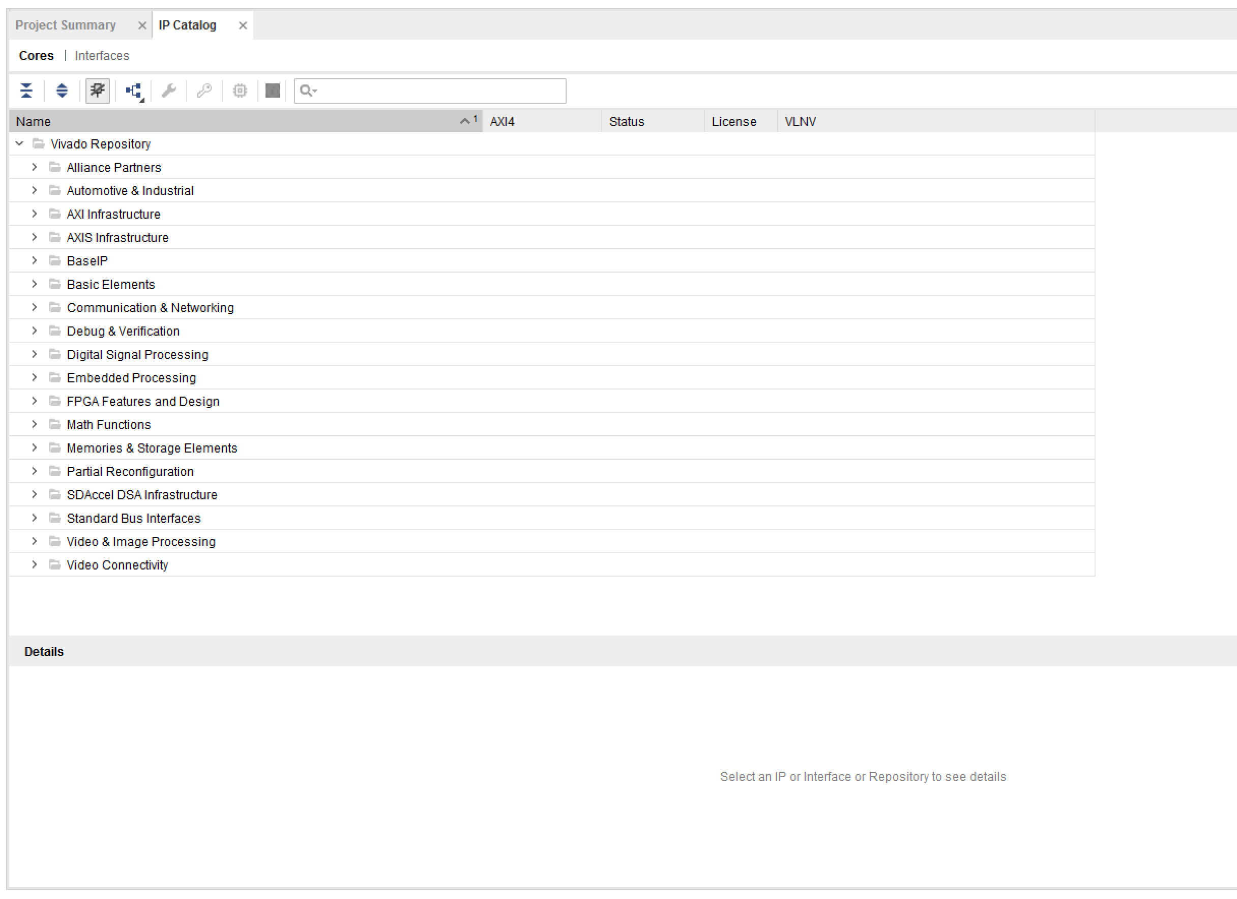
Type XADC into the search window, and it should find the "XACD Wizard".
Double click and it will run the wizard, you should see something
like this to begin:
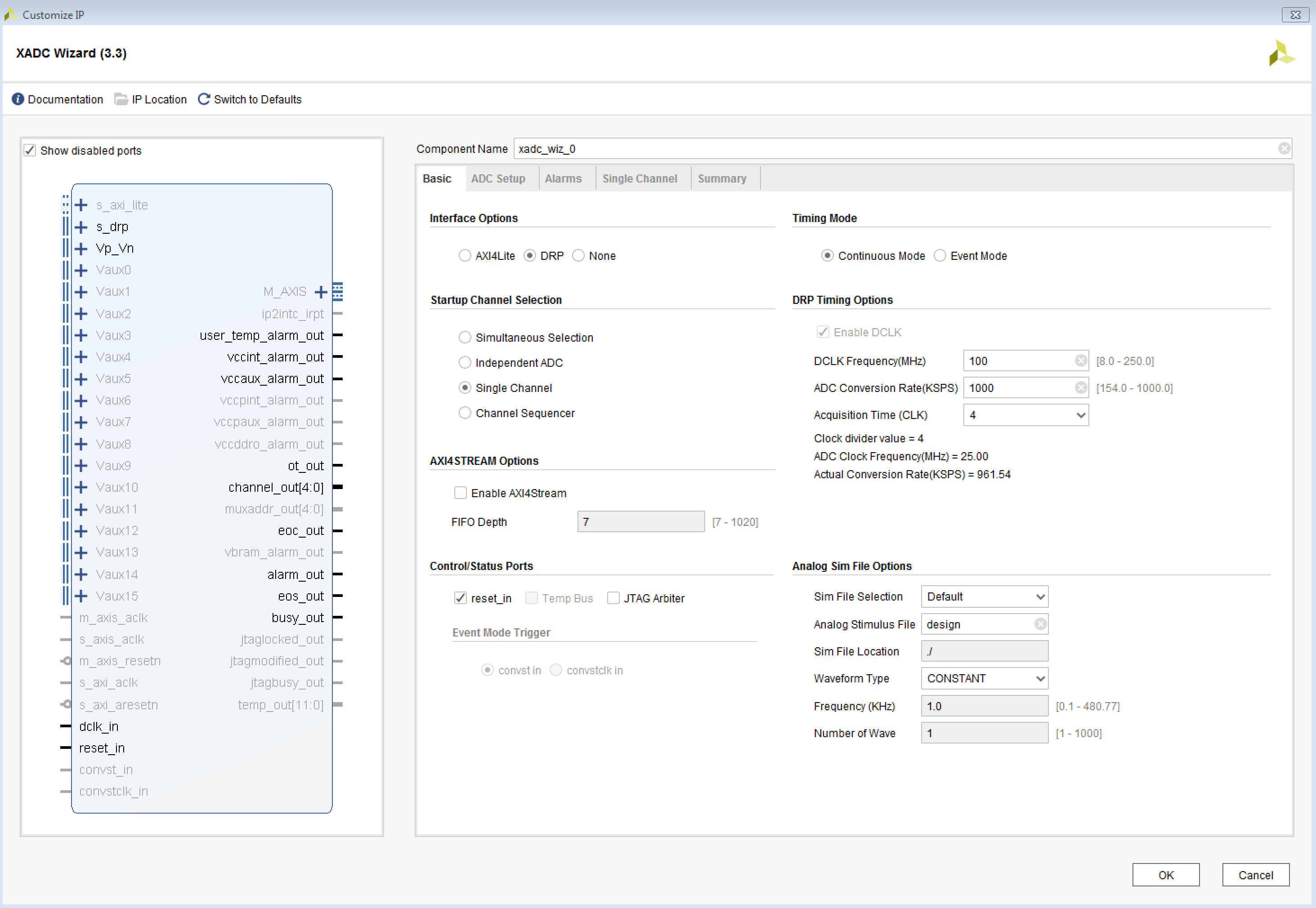
You will see a text field called "Component Name" and you will see
"xadc_wiz_0" in that field. Change it to "myxadc", and
it will show up with this name in your verilog sources panel.
Underneath "Component Name" you will see 5 tabs labeled "Basic",
"ADC Setup", "Alarms", "Single Channel", and "Summary", and these
are used to set up the instantiation. Here's what
is recommended for each of these tabs:
- Basic:
- Interface Options: DRP
- Startup Channel Selection: Single Channel
- AXI4STREAM Options: leave as is
- Control/Status Ports: deselect reset_in (not critical)
- Timing Mode: Continuous Mode
- DRP Timing Options: make sure the DCLK frequency is 104 MHz
(the remaining parameters in this block will be set for you)
- Analog Sim File Options: leave as is
- ADC Setup: leave as is
- Alarms: turn everything off by deslecting all. This is only used
when you want to read voltages and temperatures on the chip
- Single Channel: for this project we will only be driving a single
voltage into the JXADC header, so in this tab under where it
says "Select Channel" select "VAUXP6 VAUXN6",
which corresponds to J3/K3, or pins 1/7 on the header.
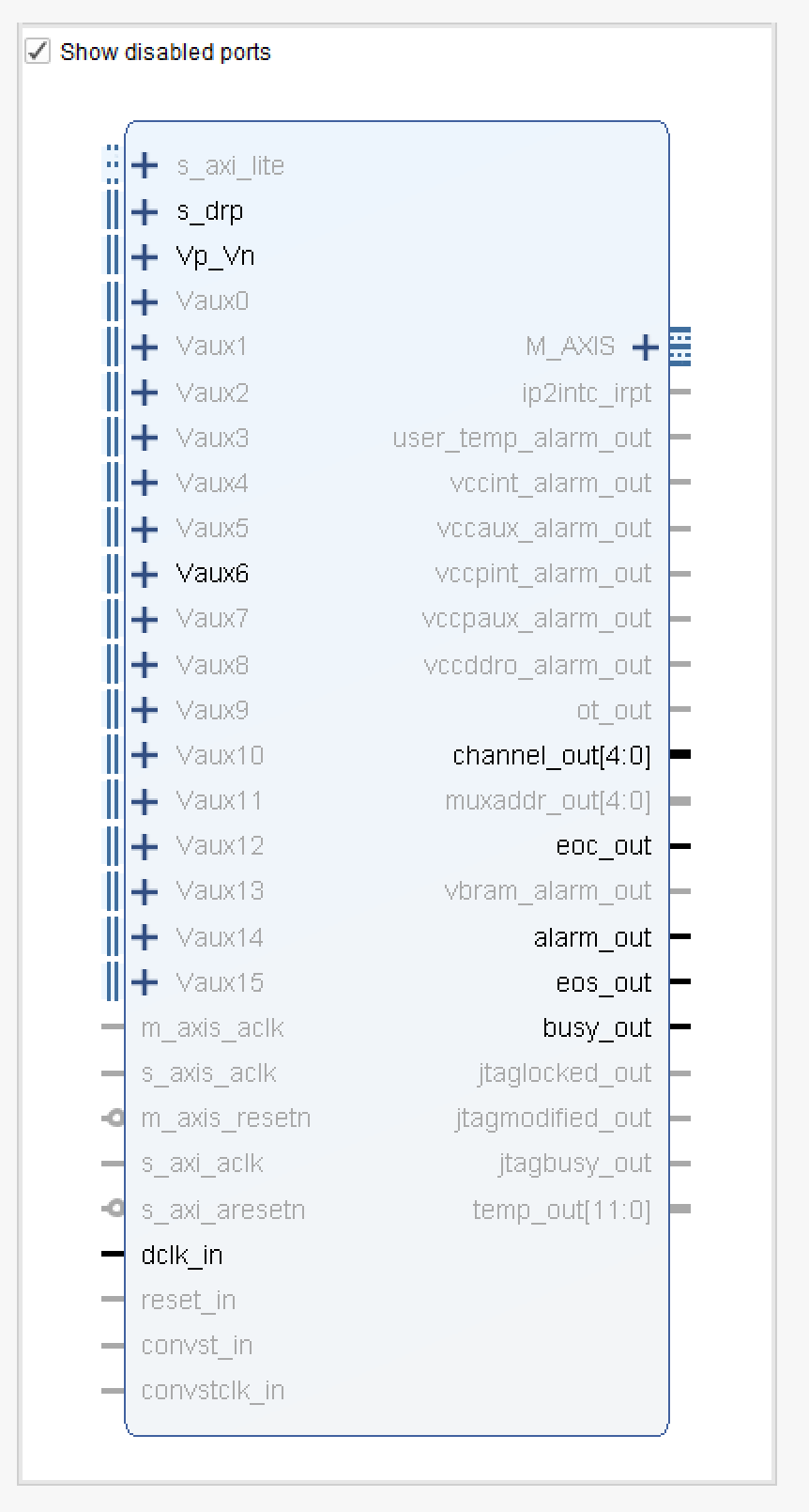
Now you are ready to generate the instantiation. You will see in the
left panel what pins will be driven, it should look like this:
Click "OK", and you should see a popup window that asks if it's ok to
create a new directory to house all of the new files. It should be
in your project directory. Click "OK". It will then pop up a window
labeled "Generate Output Product". Click "Generate", it will initiate
some activity, and at the end will inform you that it did what it was
supposed to do. Click OK.
Now you should see a new source for the XADC called myxadc
appear in the same panel with the other
sources.
If you open up what's below "myxadc" you should see a file called
"myxadc (myxadc.v)". That's your source file, it contains
the instantiation of the XADC. You can double click on it, and you will
a huge number of lines. Don't worry, all we have to do now is
instantiate myxacd and that module will do all the heavy lifting.
Here's what you do with each of these ports:
- .do_out is 16 bits from the ADC. The upper 12 bits are the data,
and the bottom 12 are status registers that we will ignore.
- .daddr_in is a pointer that tells the system what you want it
to digitize. For this project we will just look at the external
pins as analog inputs, and those are mapped to addresses 0x10-0x1F
(16 VAUX inputs). We will only be looking at pins J3/K3, which are
labeled IO_L7P_T1_AD6P_35 and IO_L7P_T1_AD6N_35 in the
mapping file as
described above. This means that
these pins are "vaux6" (it's the "AD6" in the above label that gives
it away). That means you have to set daddr_in to 0x16, or 'h16.
You can do this via a parameter, as shown below.
- .dclk_in is your system clock (50MHz here)
- .eoc_out is an output that signals the conversion is complete
- .eos_out is an output that says the sequence for latching, conversion, etc
is complete
- .den_in is the enable input. If you want this to operate continuously
then it's easy to just tie the .eoc_out line into this line
- .di_in is a 16 bit input register that you can use to set the data
explicitly, which we will not be using, so we set this to 0
- .dwe_in is set if you want to enable writing di_in, which we don't
want to do, so this is also set to 0
- .busy_out tells you if the ADC is busy (see below), so we provide a wire for it
(isbusy) but probably never need to look at it
- .alarm_out tells you if there is an alarm, which we don't care about,
so all we need to do is provide a wire
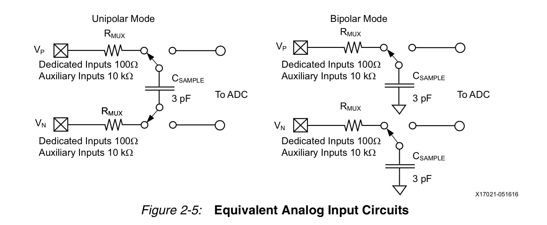
- .vp_in and .vn_in are dedicated analog input pairs that we don't care
about, so we set those to 0 as well
- .drdy_out tells you when valid data is ready to be latched
- .do_out is the actual output data, is 16 bits, but the ADC is only 12
bits so they pack the upper 12 bits of this 16 bit word with data.
The bottom 4 bits are not used (by us anyway).
- .channel_out is a 4 bit bus, but since we are using a single channel we
don't have to worry about it
For more info click on
this.
To instantiate you should place the following in your code:
//
// here is the XADC block
//
wire [6:0] daddr_in = 7'h16;
wire adc_ready, isbusy, adc_data_ready, eos_out, alarm;
wire [15:0] adc_data;
wire [4:0] channel_out;
myxadc XADC_INST (
.daddr_in(7'h16), // specifies vcaux6 pints to digitize
.dclk_in(clock104), // 50MHz clock
.den_in(adc_ready), // tied to adc_ready, tells adc to convert, tieing causes continuous conversions
.di_in(16'h0), // to set the data to something, not used here
.dwe_in(1'b0), // set to enable writing to di_in, which we don't want to do
.vauxp6(adc_p), // positive input to digitize
.vauxn6(adc_n), // negative input to digitize
.busy_out(isbusy), // tells you the adc is busy converting
.channel_out(channel_out[4:0]), // for using more than 1 channel, tells you which one. not used here
.do_out(adc_data), // adc value from conversion
.drdy_out(adc_data_ready), //tells you valid data is ready to be latched
.eoc_out(adc_ready), // specifies that the ADC is ready (conversion complete)
.eos_out(eos_out), // specifies that conversion sequence is complete
.alarm_out(alarm), // OR's output of all internal alarms, not used here
.vp_in(1'b0), // dedicated analog input pair for differential, tied to 0 if not used
.vn_in(1'b0)
);
The XADC instantiation will produce a series of configuration registers that
control how the XADC works, and you can see them in the myxadc.v
The configuration registers can be written to
and read from using the DRP (Dynamic Reconfiguration Port), which we will not
use. But it's good to see how these registers are configured, as depicted
in the list below (which comes from the verilog instantiation):
.INIT_40(16'h0016), // config reg 0
.INIT_41(16'h31AF), // config reg 1
.INIT_42(16'h0200), // config reg 2
.INIT_48(16'h0100), // Sequencer channel selection
.INIT_49(16'h0000), // Sequencer channel selection
.INIT_4A(16'h0000), // Sequencer Average selection
.INIT_4B(16'h0000), // Sequencer Average selection
.INIT_4C(16'h0000), // Sequencer Bipolar selection
.INIT_4D(16'h0000), // Sequencer Bipolar selection
.INIT_4E(16'h0000), // Sequencer Acq time selection
.INIT_4F(16'h0000), // Sequencer Acq time selection
.INIT_50(16'hB5ED), // Temp alarm trigger
.INIT_51(16'h57E4), // Vccint upper alarm limit
.INIT_52(16'hA147), // Vccaux upper alarm limit
.INIT_53(16'hCA33), // Temp alarm OT upper
.INIT_54(16'hA93A), // Temp alarm reset
.INIT_55(16'h52C6), // Vccint lower alarm limit
.INIT_56(16'h9555), // Vccaux lower alarm limit
.INIT_57(16'hAE4E), // Temp alarm OT reset
.INIT_58(16'h5999), // VCCBRAM upper alarm limit
.INIT_5C(16'h5111), // VCCBRAM lower alarm limit
The following table summarizes the configuration registers. For our purposes, since we are running
in continuous single channel mode and no alarms, only the configuration registers are important.
| Register (hex) | Value
| Name | Comments
|
|---|
| 40 | 'h0016 | config reg 0
| 4:0 selects ADC input channels, 16 means VAUX 6 only.
Settling time is 4 ticks, continuous mode,
unipolar, no external multiplexer mode,
and use averaging to calculate calibration coefficients.
|
| 41 | 'h31AF | config reg 1
| disable temperature alarms, enable ADC gain corrections, disable offset
corrections, set single channel mode
|
| 42 | 'h0200 | config reg 2
| ADCCLK = dclk_in divided by x2
|
As detailed above, the way to use the XADC is to wait for the signal adc_data_ready
to be asserted, and when it is, latch the data from the .do_out output adc_data into
what we can call r_adc_data. So we can use the following code.
//
// wait for XADC to tell you something is ready to latch
//
reg [15:0] r_adc_data;
always @ (posedge adc_data_ready)
if (reset) r_adc_data <= 16'h0;
else r_adc_data <= adc_data;
We want to use the push button to latch the adc value into the LEDs, but also
have the ADC value continuously displayed on the 4 7-segment LEDs. Let's make
a 1Hz clock for the 4 display characters to latch the values
so that the numbers don't change too fast, making it easier to see. We can use
the clock (100MHz) line and a 27-bit counter (which is approximately 108
counts) for this:
//
// make a ~1Hz clock so we can run the LED display slower
//
reg [26:0] counter;
reg [15:0] s_adc_data;
always @ (posedge clock) begin
if (reset) counter <= 0;
else counter <= counter + 1;
end
wire clock_1hz = counter[26];
always @ (posedge clock_1hz) s_adc_data <= r_adc_data;
assign display_this = version ? VERSION : s_adc_data;
Note that this is where we assign display_this.
To latch the ADC into the LEDs, we can use the debounced latch signal, which is
called latch_pulse:
//
// latching the adc value for LED output from latch pushbutton
//
reg [15:0] latched_adc; // latched adc data
always @ (posedge latch_pulse)
if (reset) latched_adc <= 0;
else latched_adc <= r_adc_data;
assign led = latched_adc;
Finally, add these lines to send some debug data out the JA and JB PMOD ports so that we
can see what the hardware is actually doing, using a logic analyzer.
//
// some output for debugging if necessary
//
assign JA = {3'b000,eos_out,adc_data_ready,adc_ready,isbusy,clock104};
assign JB = {adc_data[11:8],r_adc_data[11:8]};
Note that in the code in top.v, we will have 4 different 16-bit values for
the ADC:
- adc_data This comes right out of the XADC
block
- r_adc_data This is the value in adc_data
that is latched when adc_data_ready is asserted, so it
won't change in between assertions
- s_adc_data This is what is sent to the 7-segment
LED displays
- latched_adc This is the value in r_adc_data
when the latch push button (BTNL) is pushed, and is what is
used to drive the 16 external LEDs on the BASYS3.
Now you have to enter the pin assignments into the constraints file, which you
will first need to create. The assignments are here:
## clock
set_property PACKAGE_PIN W5 [get_ports clock]
set_property IOSTANDARD LVCMOS33 [get_ports clock]
# LEDs
set_property PACKAGE_PIN U16 [get_ports {led[0]}]
set_property IOSTANDARD LVCMOS33 [get_ports {led[0]}]
set_property PACKAGE_PIN E19 [get_ports {led[1]}]
set_property IOSTANDARD LVCMOS33 [get_ports {led[1]}]
set_property PACKAGE_PIN U19 [get_ports {led[2]}]
set_property IOSTANDARD LVCMOS33 [get_ports {led[2]}]
set_property PACKAGE_PIN V19 [get_ports {led[3]}]
set_property IOSTANDARD LVCMOS33 [get_ports {led[3]}]
set_property PACKAGE_PIN W18 [get_ports {led[4]}]
set_property IOSTANDARD LVCMOS33 [get_ports {led[4]}]
set_property PACKAGE_PIN U15 [get_ports {led[5]}]
set_property IOSTANDARD LVCMOS33 [get_ports {led[5]}]
set_property PACKAGE_PIN U14 [get_ports {led[6]}]
set_property IOSTANDARD LVCMOS33 [get_ports {led[6]}]
set_property PACKAGE_PIN V14 [get_ports {led[7]}]
set_property IOSTANDARD LVCMOS33 [get_ports {led[7]}]
set_property PACKAGE_PIN V13 [get_ports {led[8]}]
set_property IOSTANDARD LVCMOS33 [get_ports {led[8]}]
set_property PACKAGE_PIN V3 [get_ports {led[9]}]
set_property IOSTANDARD LVCMOS33 [get_ports {led[9]}]
set_property PACKAGE_PIN W3 [get_ports {led[10]}]
set_property IOSTANDARD LVCMOS33 [get_ports {led[10]}]
set_property PACKAGE_PIN U3 [get_ports {led[11]}]
set_property IOSTANDARD LVCMOS33 [get_ports {led[11]}]
set_property PACKAGE_PIN P3 [get_ports {led[12]}]
set_property IOSTANDARD LVCMOS33 [get_ports {led[12]}]
set_property PACKAGE_PIN N3 [get_ports {led[13]}]
set_property IOSTANDARD LVCMOS33 [get_ports {led[13]}]
set_property PACKAGE_PIN P1 [get_ports {led[14]}]
set_property IOSTANDARD LVCMOS33 [get_ports {led[14]}]
set_property PACKAGE_PIN L1 [get_ports {led[15]}]
set_property IOSTANDARD LVCMOS33 [get_ports {led[15]}]
##
## 7 segment display
set_property PACKAGE_PIN W7 [get_ports {segment[0]} ]
set_property IOSTANDARD LVCMOS33 [get_ports {segment[0]} ]
set_property PACKAGE_PIN W6 [get_ports {segment[1]} ]
set_property IOSTANDARD LVCMOS33 [get_ports {segment[1]} ]
set_property PACKAGE_PIN U8 [get_ports {segment[2]} ]
set_property IOSTANDARD LVCMOS33 [get_ports {segment[2]} ]
set_property PACKAGE_PIN V8 [get_ports {segment[3]} ]
set_property IOSTANDARD LVCMOS33 [get_ports {segment[3]} ]
set_property PACKAGE_PIN U5 [get_ports {segment[4]} ]
set_property IOSTANDARD LVCMOS33 [get_ports {segment[4]} ]
set_property PACKAGE_PIN V5 [get_ports {segment[5]} ]
set_property IOSTANDARD LVCMOS33 [get_ports {segment[5]} ]
set_property PACKAGE_PIN U7 [get_ports {segment[6]} ]
set_property IOSTANDARD LVCMOS33 [get_ports {segment[6]} ]
##
## LED period (dot)
set_property PACKAGE_PIN V7 [get_ports {dp}]
set_property IOSTANDARD LVCMOS33 [get_ports {dp}]
##
## digit select
set_property PACKAGE_PIN U2 [get_ports {digit[0]} ]
set_property IOSTANDARD LVCMOS33 [get_ports {digit[0]} ]
set_property PACKAGE_PIN U4 [get_ports {digit[1]} ]
set_property IOSTANDARD LVCMOS33 [get_ports {digit[1]} ]
set_property PACKAGE_PIN V4 [get_ports {digit[2]} ]
set_property IOSTANDARD LVCMOS33 [get_ports {digit[2]} ]
set_property PACKAGE_PIN W4 [get_ports {digit[3]} ]
set_property IOSTANDARD LVCMOS33 [get_ports {digit[3]} ]
## Buttons
set_property PACKAGE_PIN T18 [get_ports version]
set_property IOSTANDARD LVCMOS33 [get_ports version]
set_property PACKAGE_PIN W19 [get_ports latch]
set_property IOSTANDARD LVCMOS33 [get_ports latch]
set_property PACKAGE_PIN T17 [get_ports reset]
set_property IOSTANDARD LVCMOS33 [get_ports reset]
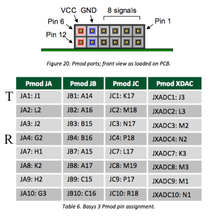
## Pmod Header JXADC
## Schematic name = XA1_P
set_property PACKAGE_PIN J3 [get_ports adc_p ]
set_property IOSTANDARD LVCMOS33 [get_ports adc_p ]
## Schematic name = XA1_N
set_property PACKAGE_PIN K3 [get_ports adc_n ]
set_property IOSTANDARD LVCMOS33 [get_ports adc_n ]
##Pmod Header JB
##Sch name = JB1
set_property PACKAGE_PIN A14 [get_ports {JB[0]}]
set_property IOSTANDARD LVCMOS33 [get_ports {JB[0]}]
##Sch name = JB2
set_property PACKAGE_PIN A16 [get_ports {JB[1]}]
set_property IOSTANDARD LVCMOS33 [get_ports {JB[1]}]
##Sch name = JB3
set_property PACKAGE_PIN B15 [get_ports {JB[2]}]
set_property IOSTANDARD LVCMOS33 [get_ports {JB[2]}]
##Sch name = JB4
set_property PACKAGE_PIN B16 [get_ports {JB[3]}]
set_property IOSTANDARD LVCMOS33 [get_ports {JB[3]}]
##Sch name = JB7
set_property PACKAGE_PIN A15 [get_ports {JB[4]}]
set_property IOSTANDARD LVCMOS33 [get_ports {JB[4]}]
##Sch name = JB8
set_property PACKAGE_PIN A17 [get_ports {JB[5]}]
set_property IOSTANDARD LVCMOS33 [get_ports {JB[5]}]
##Sch name = JB9
set_property PACKAGE_PIN C15 [get_ports {JB[6]}]
set_property IOSTANDARD LVCMOS33 [get_ports {JB[6]}]
##Sch name = JB10
set_property PACKAGE_PIN C16 [get_ports {JB[7]}]
set_property IOSTANDARD LVCMOS33 [get_ports {JB[7]}]
#Pmod Header JA
#Sch name = JA1
set_property PACKAGE_PIN J1 [get_ports {JA[0]}]
set_property IOSTANDARD LVCMOS33 [get_ports {JA[0]}]
#Sch name = JA2
set_property PACKAGE_PIN L2 [get_ports {JA[1]}]
set_property IOSTANDARD LVCMOS33 [get_ports {JA[1]}]
#Sch name = JA3
set_property PACKAGE_PIN J2 [get_ports {JA[2]}]
set_property IOSTANDARD LVCMOS33 [get_ports {JA[2]}]
#Sch name = JA4
set_property PACKAGE_PIN G2 [get_ports {JA[3]}]
set_property IOSTANDARD LVCMOS33 [get_ports {JA[3]}]
#Sch name = JA7
set_property PACKAGE_PIN H1 [get_ports {JA[4]}]
set_property IOSTANDARD LVCMOS33 [get_ports {JA[4]}]
#Sch name = JA8
set_property PACKAGE_PIN K2 [get_ports {JA[5]}]
set_property IOSTANDARD LVCMOS33 [get_ports {JA[5]}]
#Sch name = JA9
set_property PACKAGE_PIN H2 [get_ports {JA[6]}]
set_property IOSTANDARD LVCMOS33 [get_ports {JA[6]}]
#Sch name = JA10
set_property PACKAGE_PIN G3 [get_ports {JA[7]}]
set_property IOSTANDARD LVCMOS33 [get_ports {JA[7]}]
Note that the ADC value that comes out of the XADC block
(adc_data from the .do_out port) has 16 bits.
The upper 12 bits are the ADC value, the lower 4 bits are
the status. These are detailed
here.
Basically the 4 lower bits of the ADC output are telling
you something about what the ADC is doing (digitizing,
waiting, etc), which is why the lower of the 4 LED digits
is always cycling. The next 4 bits (2nd LED digit) is
also flickering, because remember the ADC is a 12 bit
number with a bit resolution of 0.244mV. So
if you put some signal into the JXADC inputs (pin 1
is positive, 7 is negative) then if it's not steady then
the lower bits of the 12-bit ADC value will flicker.
Now you should be ready to build and download the project.
What
you should see is the ADC value displayed as a 16 bit (4-digit hex)
number continuously. Push the latch button (BTNL) and the
ADC value will be displayed on the LEDs until you push it again
to get another one. If you push the version button (BTNU) then
you should get the version number displayed instead of the ADC,
which will be whatever you set it to ('h0001' here).
XADC Timing
In the above code we have brought out some signals to look at with a
logic analyzer:
assign JA = {3'b000,eos_out,adc_data_ready,adc_ready,isbusy,clock104};
assign JB = {adc_data[11:8],r_adc_data[11:8]};
This is so we can look at the actual transitions of the XADC data output
(signal adc_data) and make sure we know how to latch the data into the signal
r_adc_data.
Hook up the logic analyser
to the 8 JB outputs and 8 JA outputs.
To make sure we are exercising the XADC, we will put a voltage into
the VAUX6 inputs from a sine wave generator that has a DC offset
of 0.5V and an amplitude just under 0.5V, so that the voltage
swings the full range of the XADC, which is from 0 to 1 volt,
which should be exercising all of the 12 bits of ADC.
Then let's capture some data with the logic analyzer and
see what the actual timing looks like.
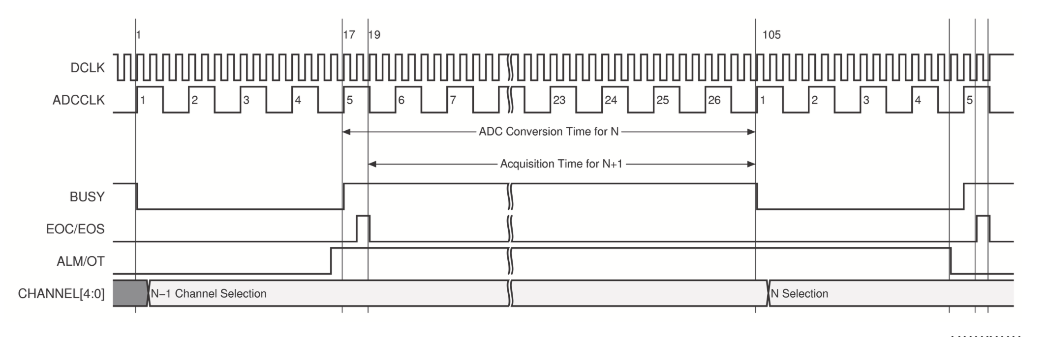
Here's what you would see:
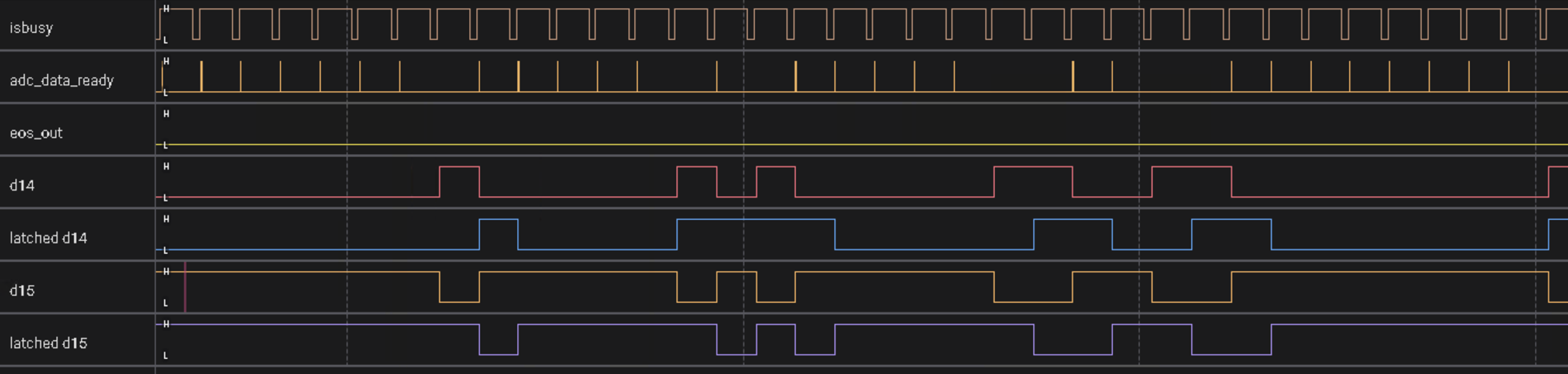
The logic analyzer is configured to show bit 14 of the XADC data
("d14") right above bit 14 of the latched data using the posedge of
adc_data_ready ("latched 14"), and the same for bit 15.
Since we are latching on the
posedge of adc_data_ready, then the value of "latched d8" should
be the same value as in adc_data in the previous XADC
conversion (that is, 1μs earlier), so "latched 15" will follow
"d15". And in the diagram, it does appear that the purple waveform
("latched 15") is ahead of the orange waveform ("d15") by 1μs.
But if you look at the 2 waveforms for bit 14, right in the middle
you see that "latched 14" does not quite follow "d14", but it does
elsewhere. This is likely a "race condition" caused by the fact
that the posedge of of "adc_data_ready" comes slightly early, when
"d14" is still high and yet to transition to it's negative value
(red waveform).
In future projects, we will want to latch the
ADC value (this is our
signal adc_data which comes out of the "do_out" port)
so that we can store the data into FIFOs and read it out later.
There are several ways to do this:
- Latch on the posedge of adc_data_ready as in the diagram above
- Latch when adc_data_ready is high
- Latch on the negedge of isbusy
Item 1 is not recommended, as the posedge of adc_data_ready is too close to
the transition edge of the data. Item 2 is also not recommendced as adc_data_ready
is very narrow compared to the clock, so this will only work when the ADC is running with
an input clock that is slow compared to the system clock used for latching. Item 3 seems
to be the safest, as it is far away from the transition edges, and we can use the edge
itself as a latch.
So I recommend that in the above code where we form the signal r_adc_data:
//
// wait for XADC to tell you something is ready to latch
//
reg [15:0] r_adc_data;
always @ (posedge adc_data_ready)
if (reset) r_adc_data <= 16'h0;
else r_adc_data <= adc_data;
that it be changed to
//
// wait for XADC to tell you something is ready to latch
//
reg [15:0] r_adc_data;
always @ (negedge isbusy)
if (reset) r_adc_data <= 16'h0;
else r_adc_data <= adc_data;
On doing so and checking with the logic analyzer, we see no discrepancy. However
the real test will come when we analyze audio signals in the RPi in some of the last
labs here.
The entire code for top.v is here:
`timescale 1ns / 1ps
module top(
    input clock,            // system clock
    input reset,            // BTNR
    input version,          // BTNU
    input latch,            // BTNL
    input adc_n, adc_p,     // VCAUX 6, P and N
    output [15:0] led,      // 16  onboard LEDs above the switches
    output [6:0] segment,   // 7-segment digit LED display
    output dp,              // "." next to each LED digit
    output [3:0] digit,     // which of the 4 digits to drive
    output [7:0] JB,        // debugging
    output [7:0] JA         //
    );
    parameter VERSION = 'h0001;
    //
    //  the XADC input clock and an internal clock divider determine the conversion
    //  rate.  we will shoot for 1MSps.  XADC takes 26 clock ticks for a conversion, so
    //  to get the input clock with a divider of 4 we multiply 4x26x1MHz = 104MHz.
    //
    //  to get such a frequency, use the Xilinx clock wizard.  let's make a 104 clock
    //  for the XADC
    //
    wire locked, clock104;
    clock_104 MYCLOCKS(
        .reset(reset),
        .clk_in1(clock),
        .locked(locked),
        .clk_out1(clock104)
    );
    //
    //  debounce the latch button
    //
    wire latch_level, latch_pulse;
    debouncer DEBOUNCE_LATCH(
        .clock(clock),
        .button(latch),
        .level(latch_level),
        .pulse(latch_pulse)
    );
    //
    //  next drive the 4 7-segment displays
    //
    wire [15:0] display_this;
    display4 DISPLAY (
        .clk100(clock),
        .number(display_this),
        .digit(digit),
        .segments(segment),
        .period(dp)
        );
    //
    //  here is the XADC block
    //
    wire [6:0] daddr_in = 7'h16;
    wire adc_ready, isbusy, adc_data_ready, eos_out, alarm;
    wire [15:0] adc_data;
    wire [4:0] channel_out;
    myxadc XADC_INST (
        .daddr_in(7'h16),   // specifies vcaux6 pints to digitize
        .dclk_in(clock104),    // 50MHz clock
        .den_in(adc_ready), // tied to adc_ready, tells adc to convert, tieing causes continuous conversions
        .di_in(16'h0),      // to set the data to something, not used here
        .dwe_in(1'b0),      //  set to enable writing to di_in, which we don't want to do
        .vauxp6(adc_p),     //  positive input to digitize
        .vauxn6(adc_n),     //  negative input to digitize
        .busy_out(isbusy),  // tells you the adc is busy converting
        .channel_out(channel_out[4:0]), // for using more than 1 channel, tells you which one.  not used here
        .do_out(adc_data),      // adc value from conversion
        .drdy_out(adc_data_ready),  //tells you valid data is ready to be latched
        .eoc_out(adc_ready),   //  specifies that the ADC is ready (conversion complete)
        .eos_out(eos_out),     //  specifies that conversion sequence is complete
        .alarm_out(alarm),      // OR's output of all internal alarms, not used here
        .vp_in(1'b0),           // dedicated analog input pair for differential, tied to 0 if not used
        .vn_in(1'b0)
    );
//
// wait for XADC to tell you something is ready to latch
//
reg [15:0] r_adc_data;
always @ (negedge isbusy)
if (reset) r_adc_data <= 16'h0;
else r_adc_data <= adc_data;
    //
    //  make a ~1Hz clock so we can run the LED display slower
    //
    reg [26:0] counter;
    reg [15:0] s_adc_data;
    always @ (posedge clock) begin
        if (reset) counter <= 0;
        else counter <= counter + 1;
        end
    wire clock_1hz = counter[26];
    always @ (posedge clock_1hz) s_adc_data <= r_adc_data;
    assign display_this = version ? VERSION : s_adc_data;
    //
    //  latching the adc value for LED output from latch pushbutton
    //
    reg [15:0] latched_adc;          // latched adc data
    always @ (posedge latch_pulse)
        if (reset) latched_adc <= 0;
        else latched_adc <= r_adc_data;
    assign led = latched_adc;
//
// some output for debugging if necessary
//
assign JA = {3'b000,eos_out,adc_data_ready,adc_ready,isbusy,clock104};
assign JB = {r_adc_data[15:12],adc_data[15:12]};
endmodule
The above project archive can be found
here.
All rights reserved. No part of this publication may be reproduced, distributed, or transmitted in any
form or by any means, including photocopying, recording, or other electronic or mechanical methods, without
prior written permission, except in the case of brief quotations embodied in critical
reviews and certain other noncommercial uses permitted by copyright law.
Unless indicated otherwise, any lecture handouts, exams, homework and exam solutions,
and the lectures themselves (including audio and video recordings) are copyrighted by
me and may not be distributed or reproduced for anything other than your personal use
without my written permission.
Last updated January, 2024