

Templating for Directed Self Assembly
By: Raymond Phaneuf
Recognizing that nature seems to be capable of producing extremely large numbers of structures at a rapid rate, a number of scientists have suggested that a solution to the problem of creating high densities on nm scale structures is self assembly. Self-assembly is not a new idea, incidently. Langmuir and Blodgett carried out experiments in self assembly in the early years of the 20th century. Crystallization, the most obvious form of self assembly has been carried out by nature shortly after the universe formed and cooled to where solidification could begin. The problem with self assembly is that you generally get only those structures that nature will provide. The ideal solution, which many researchers, including my group, are now pursuing, seems to be directed self assembly, in which a template is fabricated to guide nature in quickly assembling large arrays of structures.
 |
|
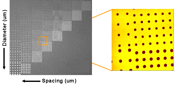
| Fig. 1. Patterned GaAs(001) surface containing arrays of cylindrical pits, 50 nm deep, with varying diameter and spacing. |
We make the template in a number of different ways-lithography followed by etching, and “nanoscraping” are the two approaches we are using at present. The first relies on depositing a “resist”, usually a polymeric film onto a surface, and then selectively changing the properties of the regions to be removed or left in place. This can be done by irradiating it through a mask with UV light, or irradiating selected regions top a scanned electron beam-both change the resistance of the polymer to being washed away by a chemical “developer.” Nanoscraping uses an atomic force microscope to selectively scrape away resist; and allows for extremely small patterns to be made. In both approaches the surface, parts of which are covered with resist, others bare, is exposed to a plasma which etches away the top layers. Finally the resist is removed chemically, leaving a clean but topographically patterned surface, a template.
The beauty of this approach is that many patterns can be explored simultaneously, allowing the effect of the pattern length scale to be explored. An example is shown in Figure 1, where we have defined pits of varying diameters and spacings onto a gallium arsenide surface. We now grow more GaAs onto this template, and observe the effect of the length scale on how new structures self-assemble during growth. We find that large period structures amplify during growth: the pits effectively grow deeper, while those whose period is below a certain characteristic size relax during growth. This characteristic size moves to larger values as we grow thicker films, and so eventually even large period structures relax, but the surface shows a transient instability. We’ve explored the temperature dependence, and find that the nature of the instability changes beneath ~540 C; rings of material form around pits during growth beneath this. We explain this change based on competing kinetic effects: one is associated with a barrier that atoms feel on difusing across a step from above, which is important at low temperatures. The second is a faster collection of atoms by larger terraces, important at high temperatures. In upcoming work, we’ll extend our patterns downward to nanometer dimensions.
 |
|
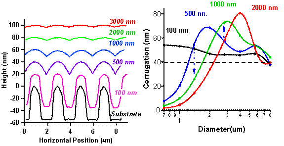
| Fig. 2. (Left) Height profiles across patterned GaAs(001) for 1 um pits spaced at 2 um, vs. thickness of grown film, (Right) with varying diameter and spacing. (right) Measured peak-valley height of patterns vs. initial diameter for different grown thicknesses. Patter lengths larger than the peak value amplify, those beneath it decay. |
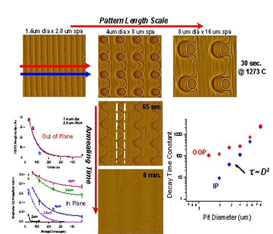
In related experiments, we have patterned stepped silicon surfaces, and measured how the length scale of our pattern affects the self assembly of bunches of steps during heating in vacuum. Beneath a characteristic length scale bunches of straight steps form, while above this the bunches form near sinusoidal shapes, with the waviness of the bunches decaying at the same rate as the height. This length scale is set both by the stiffness of the steps and their interactions.
 |
|
Fig.3. Self assembly of straight step bunches during annealing of short period patterned stepped Si(111), but wavy step bunches for long period patterns. The decay times for step bunch waviness (IP) and height (OOP) are different for small periods, but converge for large pattern structures. |
--------------------------------------------------------------------------------------------------------------------------------------------------------------------------------------------
Dr. Phaneuf is an Affiliate Associate Professor at the University of Maryland Department of Physics. He is a member of the Condensed Matter Group. Dr. Phaneuf is currently searching for two research graduate students. Any interested candidates, or for questions and comments, please contact him at phaneuf@lps.umd.edu.