In the previous Clocks and FIFOs project, we learned how to generate more complex clocks, how to use FIFOs, and how to have the RPi control asking for data and have the FPGA send it. What we want to do now is to increase the size of the FIFO so that we can buffer more data, specify a "trigger" condition for having data enter the FIFO for readout, and establish a way for the RPi to know the status of what is going on inside the FPGA.
Most oscilloscopes have the ability to continously display data, or to only display once the input signal is above some threshold (the "trigger" level). For this project, we will set a programmable threshold inside the FPGA, and when any ADC value that comes in is above that threshold, we will save a block of data that constitutes some number of points before the "trigger" so that we can see what is going on before and after triggering.
We will need to establish programmable variables inside the FPGA that the RPi can write to and read from: a trigger threshold, and the number of data points we want to save before the trigger. We will also need a control register that the RPi can write (and read from) to to control the FPGA running, and define some conventions for what each of the bits in the control register means. We will aslo need a read only (from the RPi point of view) status register inside the FPGA to tell the RPi what's happening (fifo empty, full, triggered, etc)
So the sequence of events inside the FPGA will be the following:
Note that there's a small flaw in this scheme: when the fifo is full, data taking stops until the RPi reads out everything. The inability to take date is what is known as "dead time". For this project, we won't really care about dead time, but if we were doing a real physics experiment where we wanted to measure the rate of seeing a signal such as Higgs particles in the detector, or cosmic ray muons in some scintillator paddles, we would count the number of "events" seen, divide by the data taking time, and correct for the amount of time we weren't looking ("dead time"). In such cases we want to know how much dead time there was so that we can correct for it, and in fact we would want to minimize it so that we are "live" as much as possible. This is especially true at the LHC where beam time is quite valuable!
Minimizing and measuring dead time is straight forward, although we won't be doing it in this project, mainly because we are not measuring any rates. But one way to minimize dead time is to take data continuously using multiple fifo's to store the data such that when we are reading one out, we are filling the other (or others). We could then calculate how long the readout will take, and that will tell us how deep the fifo's should be such that there would be no dead time, so that the system is always recording and always triggering.
To begin, first make a new project specifying the XC7A35T-1CPG236 chip that is in the BASYS3, and add a new toplevel verilog file (I will use top.v below). We will need the same inputs and outputs for the Clocks and FIFOs project, so top.v should start with this module declaration (setting the firmware version to 0x0001):
module top(
    input clock,            // system clock
    input reset,            // BTNR
    input version,          // BTNU
    input adc_n, adc_p,     // VCAUX 6, P and N
    input [15:0] sw,        // slide switches
    output [15:0] led,      // 16  onboard LEDs above the switches
    output [6:0] segment,   // 4 digit LED display
    output dp,              // "." next to each LED digit
    output [3:0] digit,     // 7-segment display anode select
    output reg [7:0] JB,    // PMOD JB for debugging
    output [7:0] JA,        // PMOD JA for debugging
    input rx,               // UART receive
    output tx               // UART transmit
    );
    parameter VERSION = 'h0001;
We won't be needing a debouncer here, since we aren't controlling anything critical to data taking with the push buttons.
Next we add the same clock management code we had in the previous project, which means creating the clock module by clicking "IP Catalog" search for "clock" in the IP Catalog window that pops up, and double click on "Clocking Wizard" (at the bottom of the choices). We will need 2 modules: 1 for the 25MHz and 8MHz clock and one for the 104MHz clock, just like in the previous project (for some reason Vivado won't let you generate all 3 clocks together and this might be due to how it does clock division and multiplication to get various values).
Clicking on "Clocking Wizard" opens up a "Clocking Wizard (5.4)" window. We can change the name in the "Component Name" window (I'm using "clocks"). Under the options, for "Clocking Options" leave as is but make sure that under "Input Clock Information", the Primary clock input frequency is 100.000MHz. In the "Output Clocks" tab we will need to create 2 clocks: a 25MHz clock for the uart transmission and receiver modules, and an 8MHz clock (that we will divide down to 1MHz) to manage getting data from the XADC block, which we will run at 1M samples per second. So make sure "clk_out1" and "clk_out2" are all selected, and put 25.000 for "clk_out1", 8.00 for "clk_out2". All of the rest of the tabs are ok as is, so hit "OK" and then "Generate" at the "Generate Output Products" page. This should result in a "clocks" source entry. Expand the entry, and wait until you see "clocks.v" underneath it. Double click on that to look at the ports. You should see "clk_out1", "clk_out2", and "locked" outputs and "reset" and "clk_in1". Eventually (see below),
Now go back into the IP Catalog and double click "Clocking Wizard" and generate the next clock module that will make our 104MHz clock for the XADC. Change the clock to 104.000 in the "Output Clocks" tab, and change the component name to something like "clock_104". Hit OK and Generate.
The instantiation is just like in the previous project:
     //
    //  generate a 25MHz and 8MHz clock for the UART and FIFO and 104MHz for the XADC
    //
    wire locked12, locked3, clock25, clock8, clock104;
    clocks  MYCLOCKS_1_2 (
        .reset(reset),
        .clk_in1(clock),
        .locked(locked12),
        .clk_out1(clock25),
        .clk_out2(clock8)
    );
    clock_104 MYCLOCK_3 (
        .reset(reset),
        .clk_in1(clock),
        .locked(locked3),
        .clk_out1(clock104)
    );
    //
    //  divide clock8 by 8 to get the 1MHz ADC clock
    //
    reg [2:0] count8;
    always @ (posedge clock8) count8 <= count8 + 1;
    wire clock1;
    BUFG clk1buf (.I(count8[2]), .O(clock1));
Next instantiate the display4 module to drive the 4 7-segment LED displays:
    //
    //  next drive the 4 7-segment displays
    //
    wire [15:0] display_this;
    display4 DISPLAY (
        .clk100(clock),
        .number(display_this),
        .digit(digit),
        .segments(segment),
        .period(dp)
        );
And add the uart receiver (uart_rx) and transmitter (uart_tx), using the 25MHz clock as the input clock. That means "i_Clocks_per_Bit" is 25, since we want a 1MHz bit rate (1Mbaud).
    //
    //  instantiate the UART receiver.  run with the 50MHz clock so that
    //  we can run the transmitter FSM at 100MHz and not get lost
    //
    wire dv;
    wire [7:0] rx_data;
    uart_rx RECEIVER (
        .i_Clocks_per_Bit('d25),
        .i_Clock(clock25),
        .i_Reset(reset),
        .i_Rx_Serial(rx),       // tied to FPGA rx output
        .o_Rx_DV(dv),
        .o_Rx_Byte(rx_data)
        );
    //
    //  instantiate the UART transmitter
    //
    wire tx_active, tx_done;
    wire do_transmit;
    wire [7:0] transmit_byte;
    uart_tx TRANSMITTER (
        .i_Clocks_per_Bit('d25),
        .i_Clock(clock25),
        .i_Reset(reset),
        .i_Tx_DV(do_transmit),
        .i_Tx_Byte(transmit_byte),
        .o_Tx_Active(tx_active),
        .o_Tx_Serial(tx),       // tied to FPGA tx output
        .o_Tx_Done(tx_done)
        );
And now, create the XADC block as before (see Using the FPGA ADC) and instantiate it in top.v. Let's keep the same code as in the previous project, use the 104MHz clock as the input clock, and call this myxadc:
    //
    //  here is the XADC block
    //
    wire [6:0] daddr_in = 7'h16;
    wire adc_ready, isbusy, adc_data_ready, eos_out, alarm;
    wire [15:0] adc_data;
    wire [4:0] channel_out;
    myxadc XADC_INST (
        .daddr_in(7'h16),               // specifies vcaux6 pints to digitize
        .dclk_in(clock104),                // 50MHz clock
        .den_in(adc_ready),             // tied to adc_ready, tells adc to convert, tieing causes continuous conversions
        .di_in(16'h0),                  // to set the data to something, not used here
        .dwe_in(1'b0),                  //  set to enable writing to di_in, which we don't want to do
        .vauxp6(adc_p),                 //  positive input to digitize
        .vauxn6(adc_n),                 //  negative input to digitize
        .busy_out(isbusy),              // tells you the adc is busy converting
        .channel_out(channel_out[4:0]), // for using more than 1 channel, tells you which one.  not used here
        .do_out(adc_data),              // adc value from conversion
        .drdy_out(adc_data_ready),      // tells you valid data is ready to be latched
        .eoc_out(adc_ready),            // specifies that the ADC is ready (conversion complete)
        .eos_out(eos_out),              // specifies that conversion sequence is complete
        .alarm_out(alarm),              // OR's output of all internal alarms, not used here
        .vp_in(1'b0),                   // dedicated analog input pair for differential, tied to 0 if not used
        .vn_in(1'b0)
    );
    //
    //  Wait for XADC to tell you something is ready to latch, and latch it into the
    //  r_adc_data bus. Note this means continuous latching
    //
    reg [15:0] r_adc_data;
    always @ (negedge isbusy) begin
        if (reset) r_adc_data <= 16'h0;
        else r_adc_data <= adc_data;
        end
    //
    //  make a ~1Hz clock so we can run the LED display slower
    //
    reg [19:0] counter;
    reg [15:0] s_adc_data;
    always @ (posedge clock1) begin
        if (reset) counter <= 0;
        else counter <= counter + 1;
        end
    wire clock_1hz = counter[19];
    always @ (posedge clock_1hz) s_adc_data <= r_adc_data;
    assign display_this = version ? VERSION : s_adc_data;
Note that as before, we will latch the data from the bus adc_data using the posedge of adc_data_ready, and also create a roughly 1Hz clock to latch into the LEDs so we can see in real time what the ADC is coming up with.
Next, we want to instantiate a FIFO using for ADC data using block ram that has independent read and write clocks. This brings us to consideration of how we are going to handle things like uart tx and rx, which will run with 25MHz clocks (we can't run them with 1MHz clocks since they need to be able to count to get to the middle of the 1μs bit width), and XADC which will present data at 1MHz. Below you will make a controller to take care of all of these things, but first we have to decide what clock frequency the controller will run at.
One of the main increases in functionality in this project is to be able to set a threshold for the ADC data to get written into the FIFO, and to be able to control where in the FIFO the triggered data will sit, so that when we read out the FIFO, we can see what the input is doing before and after the trigger. To do this, the controller is going to have to control the FIFO reading and writing enables. The sequence will be
We can make the fifo arbitrarily long, so instead of 1024 as in the previous project, let's make it 65536, or 16 bits of addressing. That implies that we will need a prefill register that is probably 16 bits, which means that RPi will have to send 2 bytes to fill this register (more on that below). So click on the IP Catalog, search for FIFO, click on FIFO Generator, and set it up like this:
    //
    //  instantiate our data fifo next
    //
    wire triggered;         // comes out of the controller
    wire [17:0] din = {triggered,1'b0,r_adc_data};   // feed this directly into the FIFO data input
    wire [17:0] dout;
    wire [12:0] fifo_adc_out = {dout[17],dout[15:4]};  // send to controller the ADC bits and whether this triggered
    wire wr_en;
    wire rd_en, fifo_full, fifo_empty, wr_rst_busy, rd_rst_busy;
    wire [15:0] fifo_data_count;
    adc_fifo DATA_FIFO (
        .rst(reset),
        .wr_clk(clock1),
        .rd_clk(clock1),
        .din(din),
        .wr_en(wr_en),
        .rd_en(rd_en),
        .dout(dout),
        .full(fifo_full),
        .empty(fifo_empty),
        .rd_data_count(fifo_data_count),
        .wr_rst_busy(wr_rst_busy),
        .rd_rst_busy(rd_rst_busy)
    );
Note:
wire [12:0] fifo_adc_out = {dout[17],dout[15:4]}; // send to controller the ADC bits and whether this triggered
that sends 13 bits to the controller (for output via the UART to the RPi).
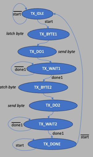
Next is the uart tx state machine, which can be just like in the Clocks and FIFOs project, with the same diagram:
The code is also the same:
    //
    //  now make a state machine to deal with transmitting 2 bytes at a
    //  time, including the FIFO value that is present.
    //
    reg [2:0] tx_state;     // 8 states so 3 bits will do
    localparam [2:0] TX_IDLE=0, TX_BYTE1=1, TX_DO1=2, TX_WAIT1=3, TX_BYTE2=4,
                    TX_DO2=5, TX_WAIT2=6, TX_DONE=7;
    reg doit;
    wire [15:0] transmit_word;
    wire begin_transfer;
    reg [7:0] tx_data;
    always @ (posedge clock25) begin
        if (reset) begin
            tx_state <= TX_IDLE;
            doit <= 0;
            tx_data <= 0;
        end
        else
            case (tx_state)
                TX_IDLE: begin
                    //
                    //  wait for begin_transfer to start
                    //
                    if (begin_transfer) tx_state <= TX_BYTE1;
                    else tx_state <= TX_IDLE;
                    doit <= 0;
                    tx_data <= 0;
                end
                TX_BYTE1: begin
                    //
                    //  latch the first byte of the transmit_word
                    //
                    tx_data <= transmit_word[7:0];
                    tx_state <= TX_DO1;
                end
                TX_DO1: begin
                    //
                    //  turn on uart_tx
                    //
                    doit <= 1;
                    tx_state <= TX_WAIT1;
                end
                TX_WAIT1: begin
                    //
                    //  turn off doit and wait for uart_tx to finish
                    //
                    doit <= 0;
                    if (tx_done) tx_state <= TX_BYTE2;
                    else tx_state <= TX_WAIT1;
                end
                TX_BYTE2: begin
                    //
                    //  latch the 2nd byte to transfer
                    //
                    tx_data <= transmit_word[15:8];
                    tx_state <= TX_DO2;
                end
                TX_DO2: begin
                    //
                    //  turn on uart_tx
                    //
                    doit <= 1;
                    tx_state <= TX_WAIT2;
                end
                TX_WAIT2: begin
                    //
                    //  wait for the 2nd byte to finish begin sent
                    //
                    doit <= 0;
                    if (tx_done) tx_state <= TX_DONE;
                    else tx_state <= TX_WAIT2;
                end
                TX_DONE: begin
                    //
                    //  wait for begin_transfer to go away
                    //
                    if (do_transmit) tx_state <= TX_DONE;
                    else tx_state <= TX_IDLE;
                end
                default: begin
                    tx_state <= TX_IDLE;
                end
            endcase
    end
    assign do_transmit = doit;
    assign transmit_byte = tx_data;
Let's beef up the UART receiving a bit to make it more bullet-proof against timing difficulties. We do this because for this project, we are going to need a more complex relationship between the FPGA and RPi, as discussed above and below (registers, etc). For instance we are going to need to have to load a register for the ADC trigger threshold, which means that the RPi will first have to send a message that says "trigger threshold is coming on the next transmission" and then have the FPGA receive the next byte and know that that byte is the threshold to save. And we don't want to have any collisions where the RPi sends data too fast and the FPGA doesn't have time to react, or if the RPi sends data too slow and the FPGA misses it. This can be easily avoided by having the uart_rx module receive data as usual, but once it receives it to put it into a FIFO, and have a controller state machine that handles UART transmissions into the FPGA just read commands/data out of the FIFO to know what to do. This is a common "buffering" scheme used in digital IO design.
We can instantiate a new FIFO that has independent read and write clocks, and use 9 bit data widths (we could use 8, since the uart rx will receive 8 bits, but the Vivado IP Catalog says that 9 bits is the closest). The depth can be kept at 1024 since memory is plentiful in the Artix-7. We won't need the "Data Counts" enabled here. Let's call this component name "rx_fifo".
The read clock will have to be 1MHz, since that is what the controller will run on. Since the write will happen when the uart RX module raises dv, which will be 1 25MHz clock tick wide, we will want to have the write clock be 25MHz, so we definitely want independent clocks so that the timing can be independent. For the fifo write enable we use dv, the signal from the uart_rx module that notifies us that a new byte has been received, and remember that the uart_rx module and the FIFO write will be using the same 25MHz clock, so that a single clock cycle of dv being asserted won't be missed by the FIFO. Then, we will have to construct a state machine that waits for rx_empty = 0 to tell it that new information is available. It will then read the fifo and process the byte received. The fifo read enable will be controlled by the same kind of state machine we used in the Clocks and FIFOs project. More on that below.
The code instantiation for the RX FIFO will look like this, and we will place this code right after the uart_rx instantiation in top.v:
    //
    //  instantiate a fifo for the UART receiving from the RPi
    //  tie rx_wr_en to dv so that we can have the fifo write clock
    //  always going.  read will be controlled by the read/write FSM.
    //  run the clocks at 25MHz to make them synchronous with the FSMs
    //
    wire rx_wr_en = dv;
    wire rx_full, rx_empty;
    wire rx_rd_en;
    wire [8:0] rx_dout;
    rx_fifo FIFO_RX  (
        .rst(reset),
        .wr_clk(clock25),
        .rd_clk(clock1),
        .din({1'b0,rx_data}),
        .wr_en(rx_wr_en),
        .rd_en(rx_rd_en),
        .dout(rx_dout),
        .full(rx_full),
        .empty(rx_empty)
    );
The state machine to handle uart receiving will have to be altered to accommodate reading and writing the new registers we will need: control, threshold, prefill, and status. To keep the code in top.v from getting too big, let's make a new module called "controller.v" and put all of the necessary registers inside it. For inputs we will need the 1MHz clock clock25, reset, the rxfifo rx_empty flag, the 8 bit rx_data byte, and the rx_rd_en fifo read enable signal. This controller also controls the TX FSM, so we will need tx_done to tell it the data has been sent, a signal that tells the TX FSM to send data (call it tx_transmit) and the 16, bits of data (call it tx_out) to send. However, remember that tx_done comes out of the uart TX module, which runs at 25MHz, so that signal will be 25ns long, however the FSM in our controller will run at 1MHz so it could (and probably would) easily miss the shorter tx_done pulse unless we "stretch" it out. So we will need to make a new module called "stretch.v" that takes an input pulse at a fast clock and stretches it out some number of ticks. The code for that could look like this:
module stretch(
    input clock,
    input reset,
    input [7:0] ticks,  // number of ticks for stretching
    input sigin,       // signal you want to stretch
    output reg sigout  // resulting stretched output
    );

    reg state;
    localparam WAIT=0, COUNT=1;
    reg [7:0] counter;
    wire done = counter == ticks;
    always @ (posedge clock) begin
        if (reset) begin
            state <= WAIT;
            sigout <= 0;
            counter <= 0;
        end
        else case (state)
            WAIT: begin
                sigout <= 0;
                counter <= 0;
                state <= sigin ? COUNT : WAIT;
            end
            COUNT: begin
                counter <= counter + 1;
                sigout <= 1;
                state <= done ? WAIT : COUNT;
            end
        endcase
    end
endmodule
It has a sigin that needs stretching, and a sigout that is
strethced, and an 8 bit value ticks that tells you how many ticks to
stretch. There's a very simple state machine that accomplishes the stretching.
Note that if you want more than 255 ticks, you can just make the input bigger,
but for our purposes, stretching a 25MHz (40ns) signal to be large enough for a
1MHz (1μs) clock to see means you need only 25 ticks. So we instantiate
this inside top.v right after the uart TX module like this:
    //
    //  note that the OUT FSM in controller waits for tx_done, which comes from uart_tx which
    //  runs with a 25HMz clock whereas this FSM here runs with a 1MHz clock
    //  (so that it can be in sync with the data fifo).  so we will need to
    //  stretch out the tx_done signal, which is only 40ns wide, to make it
    //  1us wide so the OUT FSM doesn't miss it
    //
    wire tx_done_1us;
    stretch TX_STRETCH (
        .clock(clock25),.reset(reset),.ticks('d25),.sigin(tx_done),.sigout(tx_done_1us)
    );
And we will send tx_done_1us to our controller to tell it when a byte has successfully been sent.
The controller will also need to know the value of the firmware version (16 bits), the test vector from the slide switches, maybe the r_adc_data that feeds our ADC fifo, and of course the information from the data fifo: the fifo read and write enables, the fifo empty and full flags, and the fifo read data and data counts. We might also want to send out some debug information that we can put out on the PMOD blocks for debugging with the logic analyzer.
Let's make a new source file and call it controller.v. The module declaration will therefore be something like this:
module controller(
    input clock,
    input reset,
    input rx_fifo_empty,
    input [7:0] rx_fifo_data,
    output rx_fifo_rd,
    input tx_done,
    output reg tx_transmit,
    output reg [15:0] tx_out,
    input [15:0] firmware_version,
    input [15:0] test_vector,
    input [15:0] r_adc_data,
    output data_fifo_rd_en,
    output data_fifo_wr_en,
    input data_fifo_empty,
    input data_fifo_full,
    input [12:0] data_fifo_data,        // MSB is triggered, next 12 bits are ADC
    input [15:0] data_fifo_count,
    output [15:0] led,
    output triggered,
    output [31:0] debug
    );
Note that we will be driving the 16 leds with the controller, so that we can bring the status register and other important lines out to the leds to make sure things are working ok.
This module is instantiated inside top.v like this:
    //
    //  instantiate the controller that handles uart rx, and the data fifo
    //
    wire [31:0] c_debug;
    controller CONTROL (
        .clock(clock1),
        .reset(reset),
        .rx_fifo_empty(rx_empty),
        .rx_fifo_data(rx_dout[7:0]),
        .rx_fifo_rd(rx_rd_en),
        .tx_done(tx_done_1us),
        .tx_transmit(begin_transfer),
        .tx_out(transmit_word),
        .firmware_version(VERSION),
        .test_vector(sw),
        .r_adc_data(r_adc_data),
        .data_fifo_rd_en(rd_en),
        .data_fifo_wr_en(wr_en),
        .data_fifo_empty(fifo_empty),
        .data_fifo_full(fifo_full),
        .data_fifo_data(fifo_adc_out),
        .data_fifo_count(fifo_data_count),
        .led(led),
        .triggered(triggered),
        .debug(c_debug)
        );
Note that the signal c_debug will just be a 4 byte hodge podge of signals that can be send out PMOD connectors for debugging.
The module top.v is now pretty much done except for assigning things to the JA and JB PMOD outputs. This will change over time: at the beginning you might want to debug the uart rx and tx, and later you might want to debug the controller, the fifo's etc. We only have 16 outputs for the 2 PMODs, but we can use the slide switches to tell the FPGA what signals to put out onto those connectors. We don't yet know hwat's in c_debug but at least we will be able to look at it later if we need to (see below for definitions of what the bits in c_debug mean.)
Something like the following would work, using both JA for the uart signals and JB PMOD ports for the controller signals:
    //  use the output ports JA and JB, and the slide switches to get different
    //  debug data for the logic analyzer
    //
    //  c_debug:
    //
    //
    //  2:0 rx_state
    //  3   outgoing_done
    //  4   incoming_done
    //  5   do_outgoing
    //  6   do_incoming
    //  11:7    rx_instructions
    //  15:12   in_state
    //  19:16   out_state
    //  20      tx_transmit
    //  21      out_read_fifo   which is for the ADC fifo
    //  22      in_read_fifo   which is for the rx fifo
    //  23      do_read_fifo    also for the rx fifo
    //  26:24   f_state
    //  27      df_wr_en
    //  28      df_rd_en
    //  29      count_fill
    //  30      data_fifo_empty
    //  31      data_fifo_full
    assign JA = {rx_rd_en,rx_empty,begin_transfer,tx_done,tx,dv,rx,clock25};
    always @*
        case (sw[15:14])
            2'b00: JB = {c_debug[15:12],c_debug[6],c_debug[2:0]};    // in_state,do_incoming,rx_state
            2'b01: JB = {c_debug[19:16],c_debug[5],c_debug[2:0]};    // out_state,do_outgoing,rx_state
            2'b10: JB = c_debug[31:24];     // data_fifo_full,data_fifo_empty,count_fill,rd_en,wr_en,f_state
            2'b11: JB = {c_debug[6],c_debug[5],c_debug[11:7],clock25}; //do_in,do_out,rx_instructions,clock
        endcase
The entire code for top.v including wires, registers and parameters for this first state machine can be found here.
controller.v module
We first need to figure out a convention for sending info from the RPi to the FPGA. There will be 2 types of transfers from the RPi:
There are lots of IO signals for this module based on the above details. The module input/output declaration will be the following:
module controller(
    input clock,
    input reset,
    input rx_fifo_empty,
    input [7:0] rx_fifo_data,
    output rx_fifo_rd,
    input tx_done,
    output reg tx_transmit,
    output reg [15:0] tx_out,
    input [15:0] firmware_version,
    input [15:0] test_vector,
    input [15:0] r_adc_data,
    output data_fifo_rd_en,
    output data_fifo_wr_en,
    input data_fifo_empty,
    input data_fifo_full,
    input [12:0] data_fifo_data,        // MSB is triggered, next 12 bits are ADC
    input [15:0] data_fifo_count,
    output [15:0] led,
    output triggered,
    output [31:0] debug
    );
Notice that the rx_fifo_rd line that gets tied to the RX FIFO is an output but not a reg, because we will be driving it from several different FSM's, so will be using an assign statement.
Next let's instantiate the control, threshold, and prefill registers. For the control register, we will need a bit to enable writing into the ADC FIFO, and a signal that controls whether we will be triggering (see below). For the threshold and prefill registers, we compare the 12 bits of ADC data in r_adc_data to the lower 12 bits of the threshold register, providing the trigger_start bit is enabled, and construct a line that is asserted when trigger_start is asserted and the threshold criteria is met:
    //
    //  control register.  bits are:
    //  0   set to 1 to enable writing into the data FIFO
    //  1   set to 1 to enable comparing incoming data to the trigger threshold
    //
    reg [15:0] control;
    wire global_start = control[0];
    wire trigger_start = control[1];
    //
    //  threshold and prefill registers
    //  for threshold triggering, compare the 12 bits of ADC data in r_adc_data
    //  to the bottom 12 bits of threshold
    //
    reg [15:0] threshold;
    wire trigger = trigger_start && (r_adc_data[15:4] > threshold[11:0]);
    reg [15:0] prefill;
The trigger signal tells us that the trigger has been enabled (control register bit 1), and that the data is above threshold. We use bits 15:4 of r_adc_data since that is how the XADC packs the ADC bits, and compare that value to the bottom 12 bits of the threshold register (matching bit lengths).
Next we need a state machine to sit and wait for the communication data to come into the FPGA from the RPi via the rx FIFO. Let's use the LSB of the 8-bit data byte that the RPi will send to the FPGA to tell it whether data is coming or requested (from the point of view of the RPi), and use the other 7 bits to tell it what data it is considering. We can use the convention that each data transfer is 16 bits to make things easier (and not have to handle different size transfers). So we will use LSB = 1 to mean that the RPi is going to send 16 bits of data to the FPGA, and LSB = 0 to mean that the RPi wants the FPGA to send 16 bits of data to the RPi.
RPi to FPGA
There are only 3 pieces of information the RPi needs to send: control register, threshold register, and prefill register, so we only need 2 bits to code this. Let's use bits 2:1 for this and have the following command map:
Note that we don't really need 16 bits of control register, but to make things simpler, let's make everything sent to the FPGA be 2 bytes long. For the threshold register, the ADC data is 12 bits wide so only the lower 12 bits of the threshold register will matter. For the prefill, we will use all 16 bits and note that since the fifo is 16 bits of addressing (65536 deep), then a prefill register of 16'hFFFF FFFE will put the trigger in the middle of the fifo.
FPGA to RPi
Bit 0 = 0 of the rx data byte will trigger the FPGA to send 16 bits to the RPi, and there will be 9 different data words to send: control, status, threshold, prefill, adc_data, firware version, test vector, 12-16 bits of data from the data ADC, and 16 bits of data count from the ADC. So we can have the following map (remember, the LSB=0 to tell the FPGA that the RPi wants it to send something to it):
wire fifo_last = (data_fifo_count == 16'h1);
The status register can contain as many different bits as you can fit into 16, and will go at the bottom of the controller.v code so that it can capture lots of signals:
    //
    //  status register.  bits are:
    //  0   global start enabled
    //  1   trigger start enabled
    //  2   rx fifo empty
    //  3   data fifo empty
    //  4   data fifo full
    //  5   event triggered
    //
    wire [15:0] status = {trigger,data_fifo_full,data_fifo_empty,rx_fifo_empty,trigger_start,global_start};
The status register will be a wire concatenation of relevant signals, as in the last line above.
Now we have to construct the state machine that handles reading the rx FIFO, and responding to commands and requests from the RPI. There is a lot for this FSM to do: read the rx FIFO, receive incoming data from the RPi, send out data to the RPi. That's a lot of tasks and will make for a large FSM that will be difficult to keep straight, so let's break it up into several state machines, and have all of the state machines synchronize with each other using a hard "handshake". For example, say we have 2 FSMs, labeled FSM1 and FSM2. FSM1 starts and then asserts something that tells FSM2 to start (call it start). FSM2 then does its thing and asserts a done line. FSM1 is waiting for the done line to be asserted, and when it is, it then releases start and watis for the done line to be deasserted. FSM2 is waiting for start to be deasserted before it deasserts done. When that happens, both FSM go back to the WAIT stage. This is illustrated in the figure below:
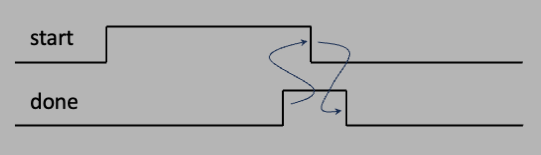
It's true that sometimes the handshake is not needed (for instance if you are sure of the timing of everything), but it's safest and makes things clear to have it.
Let's first make the state machine that controls the rx FIFO read. It will respond whenever the rx FIFO empty flag is at 0, so we can make a signal called incoming that is:
wire incoming = ~rx_fifo_empty;
When incoming is asserted, the FSM will then assert the rx fifo read enable line for 1
clock cycle and latch what comes out into a register we call
rx_instructions. Then move to a BRANCH state where it looks at the instruction
bit 0 to know if we are dealing with incoming data or request for something to be sent
back to the RPi, and depending on which one will assert a line that will start a separate
"INCOMING" and "OUTGOING" FSM to handle the two conditions.
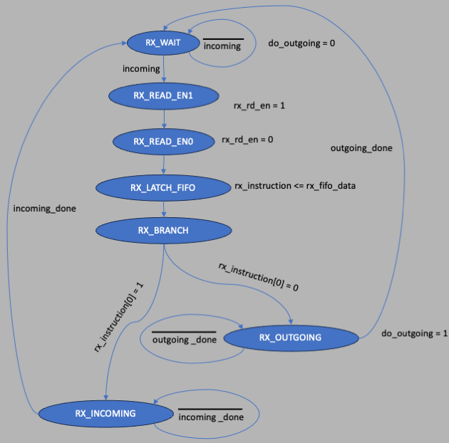
The code including wires, registers and parameters for this first state machine would look something like this:
    //
    //  here is the rx state machine, it looks at the rx fifo empty flag to know if it has
    //  anything to process
    //
    wire incoming = ~rx_fifo_empty;  // this is the signal that the fifo has something in it to process
    localparam [2:0] RX_WAIT=0, RX_READ_EN1=1, RX_READ_EN0=2,
        RX_LATCH_FIFO=3, RX_BRANCH=4, RX_INCOMING=5, RX_OUTGOING=6;
    reg [2:0] rx_state;
    reg [7:0] rx_instructions;
    reg do_read_fifo, do_incoming, do_outgoing;
    wire read_fifo_done, incoming_done, outgoing_done;
    wire branch_to_incoming = rx_instructions[0];       // incoming or outgoing
    wire [1:0] incoming_what = rx_instructions[2:1];    // what incoming is coming in
    wire [3:0] outgoing_what = rx_instructions[3:0];    // what is going out
    wire out_from_data_fifo = rx_instructions[4];
    always @ (posedge clock)
        if (reset) begin
            rx_state <= RX_WAIT;
            do_read_fifo <= 0;
            do_incoming <= 0;
            do_outgoing <= 0;
            rx_instructions <= 0;
        end
        else case (rx_state)
            RX_WAIT: begin
                rx_instructions <= 0;
                do_read_fifo <= 0;
                do_incoming <= 0;
                do_outgoing <= 0;
                rx_state <= incoming ? RX_READ_EN1 : RX_WAIT;
            end
            RX_READ_EN1: begin
                do_read_fifo <= 1;
                rx_state <= RX_READ_EN0;
            end
            RX_READ_EN0: begin
                do_read_fifo <= 0;
                rx_state <= RX_LATCH_FIFO;
            end
            RX_LATCH_FIFO: begin
                rx_instructions <= rx_fifo_data;
                rx_state <= RX_BRANCH;
            end
            RX_BRANCH: begin
                rx_state <= branch_to_incoming ? RX_INCOMING : RX_OUTGOING;
            end
            RX_INCOMING: begin
                do_incoming <= 1;
                rx_state <= incoming_done ? RX_WAIT : RX_INCOMING;
            end
            RX_OUTGOING: begin
                do_outgoing <= 1;
                rx_state <= outgoing_done ? RX_WAIT : RX_OUTGOING;
            end
            default: begin
                rx_state <= RX_WAIT;
            end
        endcase
The wires incoming_what and outgoing_what just repackage the relevant bits in the initial 8-bit data word sent from the RPi and registered in rx_instructions. The registers do_incoming and do_outgoing trigger the next 2 FSMs that handle both conditions. Again, we will use a hard handshake where this RX FSM will enter either the "RX_INCOMING" or "RX_OUTGOING" state, assert the relative lines to get things going, and wait for a done signal from each.
Next we need state machines that will process the incoming (RPi sending data to the FPGA) and outgoing (FPGA sending data to the RPi).
For the incoming FSM, all it has to do is read the FIFO again twice to get each part of the 16 bit word sent from the RPi, and then fill the right register. However, be careful, once it gets going it might have to wait for the RPi to send 2 more bytes so before reading the RX FIFO, it should wait for when the empty flag is no longer asserted. It will look like this:
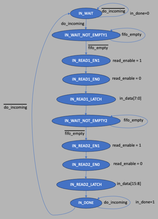
A register called in_done is used to signal the RX FSM that the incoming FSM task is complete, finishing the handshake.
The code looks like this:
    //
    //  here is the "incoming" FSM that responds to the RPi sending data to the FPGA
    //
    localparam [3:0] IN_WAIT=0, IN_WAIT_NOT_EMPTY1=1, IN_READ1_EN1=2, IN_READ1_EN0=3, IN_READ1_LATCH=4,
        IN_WAIT_NOT_EMPTY2=5, IN_READ2_EN1=6, IN_READ2_EN0=7, IN_READ2_LATCH=8, IN_DONE=9;
    reg [3:0] in_state;
    reg in_read_fifo;
    reg in_done;
    reg [15:0] in_data;
    always @ (posedge clock)
        if (reset) begin
            in_state <= IN_WAIT;
            in_read_fifo <= 0;
            in_data <= 0;
            in_done <= 0;
        end
        else case (in_state)
            IN_WAIT: begin
                in_read_fifo <= 0;
                in_data <= 0;
                in_done <= 0;
                in_state <= do_incoming ? IN_WAIT_NOT_EMPTY1 : IN_WAIT;
            end
            IN_WAIT_NOT_EMPTY1: begin
                in_state <= incoming ? IN_READ1_EN1 : IN_WAIT_NOT_EMPTY1;
            end
            IN_READ1_EN1: begin
                in_read_fifo <= 1;
                in_state <= IN_READ1_EN0;
            end
            IN_READ1_EN0: begin
                in_read_fifo <= 0;
                in_state <= IN_READ1_LATCH;
            end
            IN_READ1_LATCH: begin
                in_data[7:0] <= rx_fifo_data;
                in_state <= IN_WAIT_NOT_EMPTY2;
            end
            IN_WAIT_NOT_EMPTY2: begin
                in_state <= incoming ? IN_READ2_EN1 : IN_WAIT_NOT_EMPTY2;
            end
            IN_READ2_EN1: begin
                in_read_fifo <= 1;
                in_state <= IN_READ2_EN0;
            end
            IN_READ2_EN0: begin
                in_read_fifo <= 0;
                in_state <= IN_READ2_LATCH;
            end
            IN_READ2_LATCH: begin
                in_data[15:8] <= rx_fifo_data;
                in_state <= IN_DONE;
            end
            IN_DONE: begin
              in_done <= 1;
              case (incoming_what)
                2'b00: control <= in_data;
                2'b01: threshold <= in_data;
                2'b10: prefill <= in_data;
                2'b11: in_data <= in_data;  // should be an error condition!!!
              endcase
              in_state <= do_incoming ? IN_DONE : IN_WAIT;
            end
        endcase
    assign incoming_done = in_done;
Note that at the end, we tie the in_done register to the incoming_done
wire (we could have just declared in_done when we made the RX state machine
as well, but this is a "cleaner" way although both are fine).
Now we have to drive the output rx_fifo_read line. Since we will be reading the fifo from 2 different state machines (RX and IN), we will just use an OR and assign the value like this:
    //
    //  rx_fifo_read driver
    //
    assign rx_fifo_read = do_read_fifo | in_read_fifo;
Now we have to make the outgoing state machine that controls sending data to the RPi. All this module has to do is decode rx_instructions to know what word to latch into the bytes to send to the TX state machine that is in top.v. However, if it is going to send data from the ADC FIFO, it will have to first issue a FIFO read for 1 clock cycle and then latch the data. So the FSM will look like this:
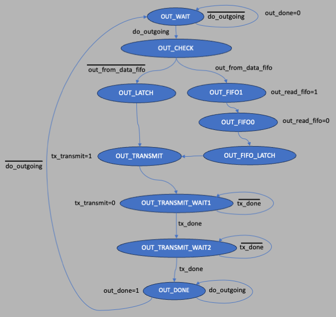
The code inside controller.v goes right after the IN FSM:
    //
    //  now make the state machine to handle sending 16 bit words to the RPi
    //
    localparam [3:0] OUT_WAIT=0, OUT_CHECK=1, OUT_LATCH=2, OUT_FIFO1=3, OUT_FIFO0=4,
        OUT_FIFO_LATCH=5, OUT_TRANSMIT=6, OUT_TRANSMIT_WAIT1=7, OUT_TRANSMIT_WAIT2=8,
        OUT_DONE=9;
    reg [3:0] out_state;
    reg out_done;
    reg out_read_fifo;
    wire fifo_last = (data_fifo_count == 16'h1);
    always @ (posedge clock)
        if (reset) begin
            out_state <= OUT_WAIT;
            tx_transmit <= 0;
            out_done <= 0;
            tx_out <= 0;
            out_read_fifo <= 0;
        end
        else case (out_state)
            OUT_WAIT: begin
                tx_transmit <= 0;
                tx_out <= 0;
                out_done <= 0;
                out_read_fifo <= 0;
                out_state <= do_outgoing ? OUT_CHECK : OUT_WAIT;
            end
            OUT_CHECK: begin
                //
                //  check if we are going to send data from the ADC FIFO
                //
                out_state <= out_from_data_fifo ? OUT_FIFO1 : OUT_LATCH;
            end
            OUT_FIFO1: begin
                //
                //  issue a fifo read and then latch the result
                //
                out_read_fifo <= 1;
                out_state <= OUT_FIFO0;
            end
            OUT_FIFO0: begin
                out_read_fifo <= 0;
                out_state <= OUT_FIFO_LATCH;
            end
            OUT_FIFO_LATCH: begin
                case (outgoing_what)
                    //
                    //  for sending back data, pack the upper 12 bits with adc value and the next 4 bits
                    //  with triggered,global_start,data_fifo_empty,fifo_last
                    //
                    //  the RPi will look at the LSB fifo_last to know if this is the last word in the fifo
                    //
                    4'b0000: tx_out <= {data_fifo_data[11:0],data_fifo_data[12],global_start,data_fifo_empty,fifo_last};
                    4'b0001: tx_out <= data_fifo_count;
                    default: tx_out <= tx_out;
                endcase
                out_state <= OUT_TRANSMIT;
            end
            OUT_LATCH: begin
//      7654 3210
//      0000 0000    control register
//      0000 0010    status register
//      0000 0100    threshold register
//      0000 0110    prefill register
//      0000 1000    r_adc_data
//      0000 1010    firmware version
//      0000 1100    test vector
                case (outgoing_what)
                    4'b0000: tx_out <= control;
                    4'b0010: tx_out <= status;
                    4'b0100: tx_out <= threshold;
                    4'b0110: tx_out <= prefill;
                    4'b1000: tx_out <= r_adc_data;
                    4'b1010: tx_out <= firmware_version;
                    4'b1100: tx_out <= test_vector;
                    default: tx_out <= tx_out;
                endcase
                out_state <= OUT_TRANSMIT;
            end
            OUT_TRANSMIT: begin
                tx_transmit <= 1;
                out_state <= OUT_TRANSMIT_WAIT1;
            end
            OUT_TRANSMIT_WAIT1: begin
                tx_transmit <= 0;
                out_state <= tx_done ? OUT_TRANSMIT_WAIT2 : OUT_TRANSMIT_WAIT1 ;
            end
            OUT_TRANSMIT_WAIT2: begin
                out_state <= tx_done ? OUT_DONE : OUT_TRANSMIT_WAIT2;
            end
            OUT_DONE: begin
                out_done <= 1;
                out_state <= do_outgoing ? OUT_DONE : OUT_WAIT;
            end
        endcase
    assign outgoing_done = out_done;
So if the RPi is asking for data from the ADC FIFO, this FSM will branch off in the "OUT_CHECK" state to the "OUT_FIFO1" state, issue the read enable for 1 clock cycle and then latch the data in the "OUT_FIFO_LATCH" state. If the RPi is not asking for such data, it goes from the "OUT_CHECK" into the "OUT_LATCH" state, and latches the relevant data. From either the "OUT_LATCH" or the "OUT_FIFO_LATCH", it goes into the "OUT_TRANSMIT" state and waits for the TX FSM (which is inside top.v) to finish by waiting for two successful tx_done signals from the uart_tx module, asserts out_done and then waits for do_outgoing to go away before going back into "OUT_WAIT".
The last thing we need to do is implement a state machine that will control what is inside the ADC FIFO. The easiest thing to do is to just keep the FIFO enable asserted and let all ADC data go into it, but then it will fill up and stop. And if we wanted a trigger condition applied, we'd have to keep reading it out and letting it fill up until we spotted the trigger condition. Not very efficient! So what we can do instead is have the FSM use the prefill register, and when the global_start (from the control register) is asserted, keep the FIFO read enable high until the number of words in the FIFO is equal to the prefill register value. When that happens, it will then start reading the FIFO on evey clock tick, so that the total number of words in the FIFO stays at the prefill value. When we get the trigger, it will then stop reading the FIFO and let it fill up. The ADC value that caused the trigger will then be at the prefil value, and when the FIFO is full, it deasserts the write enable and waits for a reset condition (for instance it could wait for the ADC FIFO to be empty again after the RPi reads it out).
The FSM looks like this:
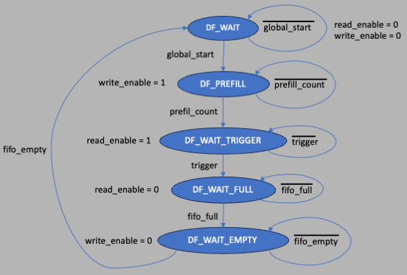
And the code would be:
    //
    //  here is a state machine that takes care of filling the data fifo
    //
    reg [2:0] f_state;
    localparam [2:0] DF_WAIT=0, DF_PREFILL=1, DF_WAIT_TRIGGER=2,
        DF_WAIT_FULL=3, DF_WAIT_EMPTY=4, DF_READ1=5, DF_WAIT_ACK=6;
    reg df_rd_en, df_wr_en;
    reg [15:0] count_fill;
    wire counted = count_fill == prefill;
    always @ (posedge clock) begin
        if (reset) begin
            count_fill <= 0;
            df_rd_en <= 0;
            df_wr_en <= 0;
            f_state <= DF_WAIT;
        end
        else case (f_state)
            DF_WAIT: begin
                //
                //  wait for global_start
                //
                count_fill <= 0;
                df_rd_en <= 0;
                df_wr_en <= 0;
                f_state <= global_start ? DF_PREFILL : DF_WAIT;
            end
            DF_PREFILL: begin
                //
                //  prefill number of data equal to value of prefill register
                //  this means prefill should never be zero!
                //  prefill means enable write but not read
                //
                df_wr_en <= 1;
                count_fill <= count_fill + 1;
                f_state <= counted ? DF_WAIT_TRIGGER : DF_PREFILL;
            end
            DF_WAIT_TRIGGER: begin
                //
                //  prefill reached.  start reading on every clock tick so that
                //  the number of words remains constant.  then wait for a
                //  trigger
                //
                df_rd_en <= 1;
                f_state <= trigger ? DF_WAIT_FULL : DF_WAIT_TRIGGER;
            end
            DF_WAIT_FULL: begin
                //
                //  trigger!   stop reading and wait for the fifo to fill up
                //
                df_rd_en <= 0;
                f_state <= data_fifo_full ? DF_WAIT_EMPTY : DF_WAIT_FULL;
            end
            DF_WAIT_EMPTY: begin
                //
                //  fifo is full. wait for it to be emptied via UART.  here is where
                //  we also have to control the fifo read enable, waiting for a signal
                //  from rx_state to read 1 data from the fifo
                //
                df_wr_en <= 0;
                f_state <= data_fifo_empty ? DF_WAIT : DF_WAIT_EMPTY;
            end
            default: begin
                count_fill <= 0;
                df_rd_en <= 0;
                df_wr_en <= 0;
                f_state <= DF_WAIT;
            end
        endcase
    end
    assign data_fifo_wr_en = df_wr_en;
    assign data_fifo_rd_en = out_read_fifo | df_rd_en;
We also want to drive the led outputs, so let's use this to allow us to see what we are doing by looking at the leds:
    //
    //  drive the output led signals
    //
    //  0       global_start
    //  1       trigger_start
    //  2       data_fifo_empty
    //  3       data_fifo_full
    //  6:4     rx_state
    //  9:7     f_state
    //  14:10   rx_instructions
    assign led = {1'b0,rx_instructions[4:0],f_state[2:0],rx_state[2:0],
                data_fifo_full,data_fifo_empty,trigger_start,global_start};
And lastly, drive the debug output so that top.v can send information to the PMOD
for debugging:
    //
    //  2:0 rx_state
    //  3   outgoing_done
    //  4   incoming_done
    //  5   do_outgoing
    //  6   do_incoming
    //  11:7    rx_instructions
    //  15:12   in_state
    //  19:16   out_state
    //  20      tx_transmit
    //  21      out_read_fifo   which is for the ADC fifo
    //  22      in_read_fifo   which is for the rx fifo
    //  23      do_read_fifo    also for the rx fifo
    //  26:24   f_state
    //  27      df_wr_en
    //  28      df_rd_en
    //  29      counted
    //  30      data_fifo_empty
    //  31      data_fifo_full
    assign debug = {data_fifo_full,data_fifo_empty,counted,df_rd_en,df_wr_en,    //31:27
        f_state[2:0],do_read_fifo,in_read_fifo,out_read_fifo,tx_transmit,           //26:20
        out_state[3:0],in_state[3:0],rx_instructions[4:0],                          //19:7
        do_incoming,do_outgoing,incoming_done,outgoing_done,rx_state[2:0]};         //6:0
The code for controller.v can be found here.
Lastly, add the constraints, they should be the same as in the previous project Clocks and FIFOs
Our project should be complete. You should have top.v, controller.v, stretch.v, and the usual files uart_rx.v, uart_tx.v, display4.v, and segnum.v. The above project archive can be found here.
Next we will write some tkinter python code to make things happen on the RPi.
RPi Python code
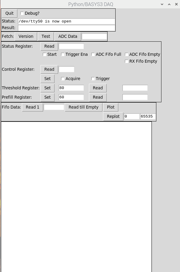
You can see a version of the code that allows you to talk to the FPGA and read out the ADC FIFO here. It is very similar to the previous tkinter program, but has the new addressing scheme. It also and assumes every data transmitted or received is 16 bits (2 bytes), which means you have to take a 16 bit integer and chop it up into 2 bytes and send each byte one at a time in "little endian" order, which means low byte first, high byte second.
Starting from the top, the "debug" checkbox when checked will cause a lot of printout to the terminal. The program automatically opens the serial port /dev/ttyS0, so if you redownload into the FPGA, you will have to quit and restart this code to get the connection to the FPGA updated (or modify the code and add a button to close and reopen the serial connection). The next line ("Fetch") has buttons that will read the firmware version, the slide switches ("Test"), and the ADC data right out of the XADC latched value r_adc_data. Note that when you hit "ADC Data", it puts the full 16 bit word in the window to the right of the button, and that word will have the ADC value in the upper 12 bits (so the lowest hex character will not be part of the ADC), but in the "Result" window above, it will strip off the ADC value and type it there.
The "Status Register" is a read-only register. Which you click "Read", it will read the register from the FPGA, put the value in the text windown next to the button, and decode and fill in the check boxes below ("Start", "Trigger Ena", etc). The "Control Register" has a "Read" button that has the same function as the "Status Register", but so far there are only 2 bits in the Control Register that matter: global_start ("Acquire") and trigger_start ("Trigger"). If you check either and of these 2 bits and hit "Set", the program writes into the control register accordingly. Note that you can't set the bits one at a time: each "Set" will write a full control register word, wiping out what was there before the transfer.
The next 2 lines allow you to "Set" and "Read" the threshold register and the prefill register. The text windows are interpreted as hex values (you can easily change this in code if you like). What you might do to set the threshold value is read the "ADC Data" from the top to see what the ADC is seeing, and set the threshold value accordingly.
The program looks like this when you run it:
The process for setting up should be something like the following:
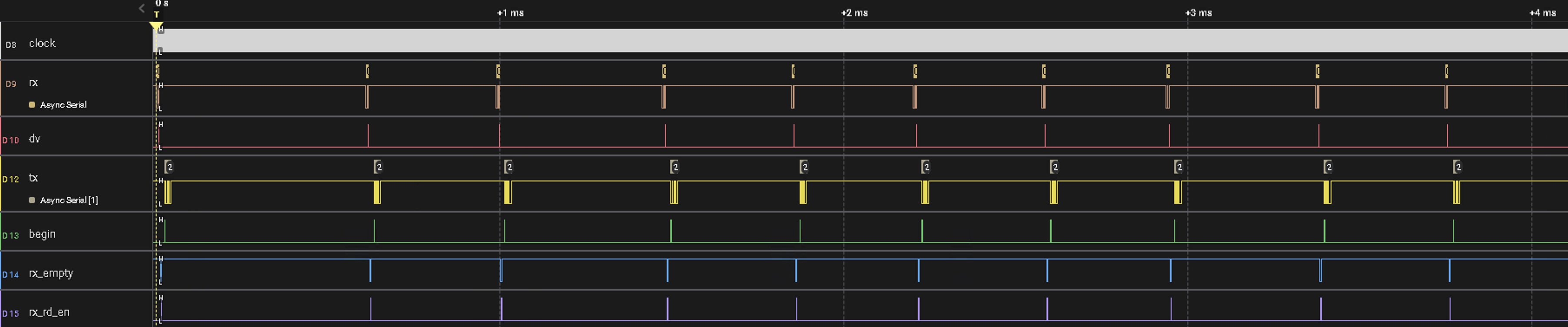
The next figure shows the timing for reading a single data word from the FIFO.
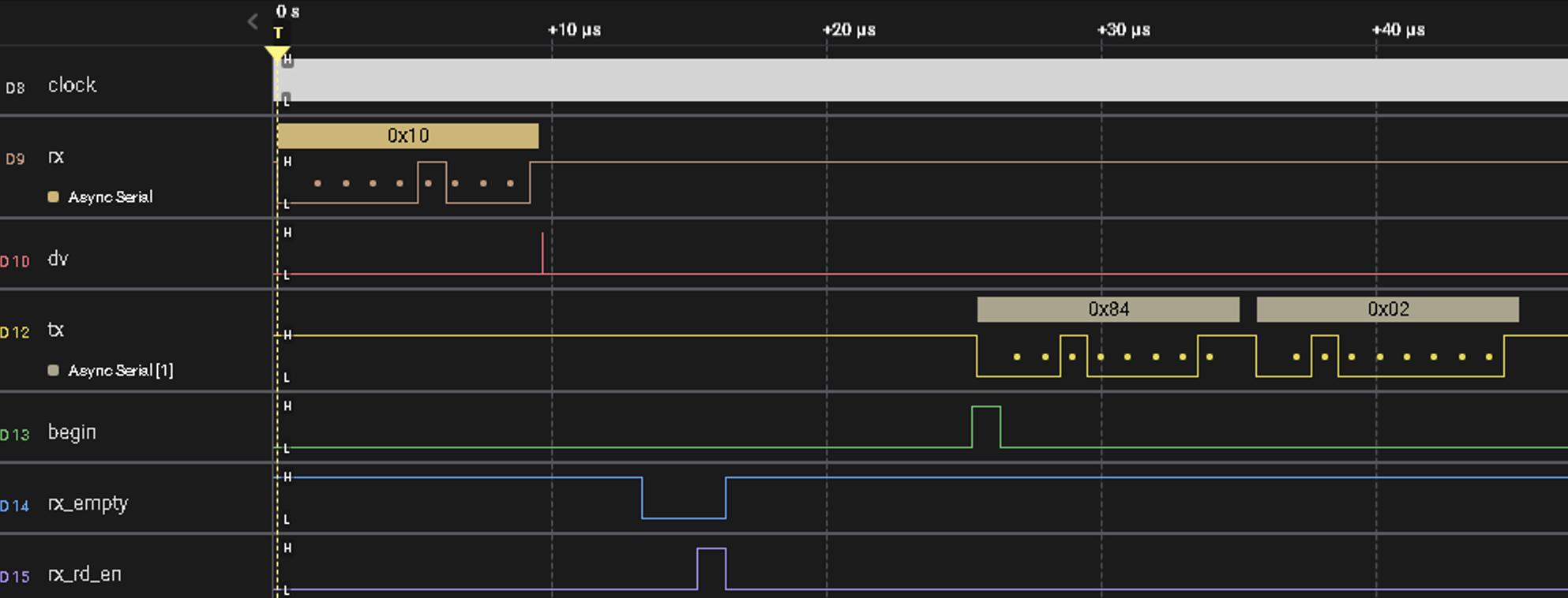
The clock is at 25MHz, or 40ns period, and the logic analyzer scale is showing 10s of μs so the clock signal looks like a solid white band. The next signal is the rx line, and you can see the transition. The logic analyzer reports that the byte sent is 0x10, which is the correct address to ask for a data word from the ADC FIFO. Line 14 is rx_empty, which is what the RX FSM waits for to know there's something to be read from the FIFO. You can then see rx_rd_en go high. The RX FSM then decodes it and causes 16 bits to be read from the ADC FIFO (not shown), and then begins a 2 byte transfer which can be seen in line 12 tx. So the time between the start of the request by the RPi to get a data word to the end of the transfer takes around 45μs.
In the next figure we see what 10 transfers look like in time.
The resolution in the screen shot is not so great, but the 10 transfers take around 4.5ms, or around 450μs per transfer. Most of the time here is taken up inside the RPi, probably just the slowness of Python. So if each transfer takes around 400μs and we have 65535 words, then it takes around 26s to read the entire FIFO. This can probably be sped up by optimzing Python. Anyway after the data is transfered, the Python program draws a plot by hand in the canvas. It will be left as an exercise to the student to make use of pyplot or some other such plotting program to make a nicer plot than the one in the screen shot below:
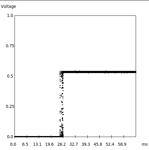
Note that the prefill value is 0x6000, which is around 25k hex, and the FIFO is filled every 1μs so the transition is in the right place, around 25ms. The fact that it is not sharp is due to the bouncing. You can blow this plot up using "Replot" and setting the limits correctly to look at the edge:
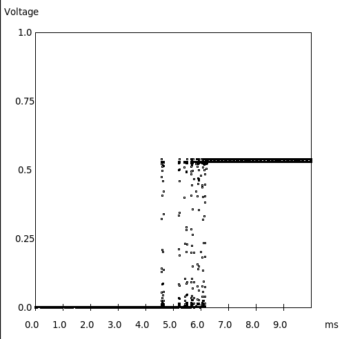
and you can clearly see the bouncing where I pushed down on the button to change the voltage from 0 to around 0.6 Volts.