As we have seen with the ADC tutorial, Vivado has the ability to generate functional blocks via it's "IP Catalog". In this lab we will learn to generate 2 more important gadgets: the clock generator, and the FIFO, which stands for "first in first out".
First let's start a new project that will use the XADC voltmeter capability, have the transfers initiated by the RPi, but with clock generation.
We already know how to take a system clock and divide it by any arbitrary power of 2 using DFFs, and to put that clock on a high quality low impedance clock line internally (BUFG). The Artix 7 series has the circuitry to enable generating a clock that has pretty much any frequency you desire, as long as the ratio of the output clock to the input clock is a rational number. That is, it can multipy and divide a clock by some integer.
For the toplevel top.v module we will need the same inputs as in the Voltmeter 2 project:
module top(
    input clock,    // system clock
    input reset,    // BTNR
    input version,  // BTNU
    input adc_n, adc_p, // VCAUX 6, P and N
    input [15:0] sw,    // slide switches
    output [15:0] led,  // 16  onboard LEDs above the switches
    output [6:0] segment,   // 4 digit LED display
    output dp,              // "." next to each LED digit
    output [3:0] digit,
    output [7:0] JB,
    output [7:0] JA,
    input rx,               // UART receive
    output tx               // UART transmit
    );
    parameter VERSION = 'h0001;
Next let's add the debouncer for the reset and version push buttons (we won't need any others for this project).
    //
    //  debounce the reset and version buttons
    //
    wire reset_level, reset_1s;
    debouncer DEBOUNCE_RESET(
        .clock(clock),
        .button(reset),
        .ticks(17'd25000),      // 25k x 40ns = 1ms
        .level(reset_level),
        .pulse(reset_1s)
    );
    wire version_level, version_1s;
    debouncer DEBOUNCE_VERSION(
        .clock(clock),
        .button(version),
        .ticks(17'd25000),      // 25k x 40ns = 1ms
        .level(version_level),
        .pulse(version_1s)
    );
We are going to need quite a few clocks here:
Click on IP Catalog and search for "clock" and you should see "Clocking Wizard" at the bottom. Double click and to open it. In the pop-up window, change the component name to "clock_8_25". The clocking options tab can be left as is, with the primary clock set at 100MHz as a default. Click on the "Output Clock" tab, you should see a list of "Output Clock" in the first column with only the first one checked. Let's generate 2 clocks: 1 for the UART (25MHz as before), and one for the FIFO that we will write data from the XADC into, which should be at 1MHz since that's how fast we are digitizing. So for "clk_out1" put in 25.000 for the requested freqency and check "clk_out2" and put in 1.000. You will see a red warning, and some verbiage that says you can't use 1.0. What's happening is that this module can't synthesize a clock that is 100 times the period as the input clock, in fact the smallest frequency it can generate is 8MHz. So change it to 8.0 and it should be happy (this is for Vivado 2023.1, if you are running a more recent version then maybe it will work at 1.0). Hit OK at the bottom and "Generate" at the "Generate Output Products" popup window and it should put another source in the Sources window called clock_8_25(clock_8_25.xcl).
Next do the same thing to generate the 104MHz clock, call this module "clock_104", and change the "Output Clock" to 104.000 and hit OK and generate.
Now we have to instantiate both modules in top.v to get all 3 new clocks:
    //
    //  generate a 25MHz and 8MHz clock for the UART and FIFO and a 104MHz clock for the XADC
    //  so that we can digitize at 1MSps
    //
    wire locked12, locked3, clock25, clock8, clock104;
    clock_8_25 MYCLOCKS12 (
        .reset(reset_1s),
        .clk_in1(clock),
        .locked(locked12),
        .clk_out1(clock25),
        .clk_out2(clock8)
    );
    clock_104 MYCLOCK3 (
        .reset(reset_1s),
        .clk_in1(clock),
        .locked(locked3),
        .clk_out1(clock104)
    );
    //
    //  divide clock8 by 8 to get the 1MHz ADC clock
    //
    reg [2:0] count8;
    always @ (posedge clock8) count8 <= count8 + 1;
    wire clock1;
    BUFG clk1buf (.I(count8[2]), .O(clock1));
The first few lines instantiates the MYCLOCK module, with a 25MHz,
8MHz, and 104MHz output. The next few makes a 3 bit counter that can count to 8,
and uses the MSB, which transistions at 1MHz, and puts it out a BUFG to
make a good clock.
Next the usual: LED display and the UART rx and tx drivers:
    //
    //  next drive the 4 7-segment displays
    //
    reg [15:0] r_adc_data;
    wire [15:0] display_this;
    display4 DISPLAY (
        .clk100(clock),
        .number(display_this),
        .digit(digit),
        .segments(segment),
        .period(dp)
        );
    //
    //  instantiate the UART receiver.  run with the 50MHz clock so that
    //  we can run the transmitter FSM at 100MHz and not get lost
    //
    wire dv;
    wire [7:0] rx_data;
    uart_rx RECEIVER (
        .i_Clocks_per_Bit('d25),
        .i_Clock(clock25),
        .i_Reset(reset),
        .i_Rx_Serial(rx),       // tied to FPGA rx output
        .o_Rx_DV(dv),
        .o_Rx_Byte(rx_data)
        );
    //
    //  instantiate the UART transmitter
    //
    wire tx_active, tx_done;
    wire do_transmit;
    wire [7:0] transmit_byte;
    uart_tx TRANSMITTER (
        .i_Clocks_per_Bit('d25),
        .i_Clock(clock25),
        .i_Reset(reset),
        .i_Tx_DV(do_transmit),
        .i_Tx_Byte(transmit_byte),
        .o_Tx_Active(tx_active),
        .o_Tx_Serial(tx),       // tied to FPGA tx output
        .o_Tx_Done(tx_done)
        );
Note that the input to the LED display is the signal display_this
which is driven below.
We will need an XADC block, so make that next using the IP Catalog, search for XADC, and double click on XADC Wizard. Change the name to XADC_IP in the Component Name window, and deselct reset_in in the Basic tab and leave the DCLK at 100MHz. Leave the ADC Setup tab as is, and deselect everything in the Alarms tab. In the Single Channel tab, chnage the Select Channel to VAUP6 VAUN6 and hit OK and then Generate. If you get a popup that says "Out-of-context module run was launched for generating output products" just hit ok, it's just informational.
Then instantiate it inside top.v like this:
    //
    //  here is the XADC block
    //
    wire [6:0] daddr_in = 7'h16;
    wire adc_ready, isbusy, adc_data_ready, eos_out, alarm;
    wire [15:0] adc_data;
    wire [4:0] channel_out;
    XADC_IP XADC_INST (
        .daddr_in(7'h16),   // specifies vcaux6 pints to digitize
        .dclk_in(clock104),    // 50MHz clock
        .den_in(adc_ready), // tied to adc_ready, tells adc to convert, tieing causes continuous conversions
        .di_in(16'h0),      // to set the data to something, not used here
        .dwe_in(1'b0),      //  set to enable writing to di_in, which we don't want to do
        .vauxp6(adc_p),     //  positive input to digitize
        .vauxn6(adc_n),     //  negative input to digitize
        .busy_out(isbusy),  // tells you the adc is busy converting
        .channel_out(channel_out[4:0]), // for using more than 1 channel, tells you which one.  not used here
        .do_out(adc_data),      // adc value from conversion
        .drdy_out(adc_data_ready),  //tells you valid data is ready to be latched
        .eoc_out(adc_ready),   //  specifies that the ADC is ready (conversion complete)
        .eos_out(eos_out),     //  specifies that conversion sequence is complete
        .alarm_out(alarm),      // OR's output of all internal alarms, not used here
        .vp_in(1'b0),           // dedicated analog input pair for differential, tied to 0 if not used
        .vn_in(1'b0)
    );
If you look at page 75 of the
XADC document
where it discusses timing, you will see this figure:
    //
    //  wait for XADC to tell you something is ready to latch. note this means continuous latching.
    //
    reg [15:0] r_adc_data;
    always @ (negedge isbusy) begin
        if (reset) r_adc_data <= 16'h0;
        else r_adc_data <= adc_data;
        end
    //
    //  make a ~1Hz clock so we can run the LED display slower
    //
    reg [19:0] counter;
    reg [15:0] s_adc_data;
    always @ (posedge clock1) begin
        if (reset_1s) counter <= 0;
        else counter <= counter + 1;
        end
    wire clock_1hz = counter[19];
    always @ (posedge clock_1hz) s_adc_data <= r_adc_data;
    assign display_this = version_level ? VERSION : s_adc_data;
We also want to drive the input to the 7 segment LED display to show the ADC value coming out of XADC, but if we use r_adc_data, it will switch at 1MHz and the LED signal will be hard to see. So we can construct a 20-bit counter (20 bits is roughtly 1M) to divide the 1MHz clock down to 1Hz and latch r_adc_data into a new 16-bit register called s_adc_data, and feed that new register into display_this.
If you look at the 7 Series FPGA Overview on page 3 it tells you that the chip we are using, the XC7A35T, has 400 kbits of distributed RAM (these are the LUTs that the FPGA uses for logic) and up to 1.8Mbit of "block ram", which is ram that is just there for storing data. The 1.8Mbits can be configured for blocks of data that have different "widths" (number of bits per memory word) and "depths" (number of memory words). For instance, you can configure it as just a large 1.8Mbit storage of single bits, or you can configure it as 900k words that have 2 bit depth. On page 9 of that document where it discusses BLOCK RAM, you can see that each buffer can be configured as (width×depth) 1×32k, 2×16k, 4×8k, 9×4k, 18×2k, 36×1k, and 72×512. The XC7A35T has 100 of these blocks to use, which is plenty for us.
For our purposes, since we need 16 bit words from the XADC block, we will use the 18×2k. For our XADC system, we have a 12 bit ADC, which packs data into a 16 bit word. The 16 bits are described on page 25 of ug480_7Series_XADC.pdf:
The data are packed in the upper 12 bits, with the bottom 4 being used for averaging and other effects to improve the resolution. We won't be using those bottom 4 bits, so we can store them in our 18-bit wide buffer or we can use the extra 6 bits of the 18-bit word to send messages to the RPi, such as "keep reading" or "stop reading" or "this particular word is the trigger" and so on.
Now, let's make a FIFO. We want a FIFO that can be written into with a 1MHz clock, since that is the conversion time for the XADC. And, we want to read it out with a clock that's convenient. Note that we will read this FIFO out and send the data to the RPi, 16 bits at a time. So the FSM that controls sending data to the RPi will also control the FIFO. We used the clock25 for that so that we can see things clearly on the logic analyzer, so we will use the same clock25 to drive the FIFO read clock.
FIFOs are controlled by enables. There's a write enable, and a read enable. FIFOs also have information signals that are very useful, particularly a wire that says whether the FIFO is full, and one that says whether it's empty. These wires are updated by the synchronous circuitry inside the FIFO, which happens at the posedge of the input clock, so if you need these infomational signals (which we do), then you need to have the read and write clocks always running (the fifo empty flag is updated on the read clock, and the fifo full flag on the write clock).
Make a FIFO by clicking on IP Catalog and searching for FIFO, and clicking on FIFO Generator. That will pop up a window that allows you to configure your FIFO. Let's call this FIFO_DATA in the component window. In the Basic tab change the Fifo Implementation option from "Common Clock Block RAM" to "Independent Clocks Block RAM". That will give us a FIFO that lives in the block ram, with independent read and write clocks. Everything else in that tab is ok. In the Native Ports tab, you will see that you can change the width of the FIFO. Width means how many bits are stored in each FIFO memory location. We want it to be 18 (16 is not allowed), and let's make the FIFO 1024 (10 bits) deep so that we can see a large number of hits. Everything else is as is. Leave everything as is in the Status Flags tab, but in the Data Counts tab, let's enable "Read Data Count" and leave the width at 16 bits. This means that when we read the FIFO, we can know how many words are left. It will come in handy in future projects.
Click OK and then "Generate" in the next window, and FIFO_DATA will appear in the Souces window under top.v. Then, instantiate this inside top.v like this:
    //
    //  instantiate our fifo next
    //
    wire [17:0] din = r_adc_data;   // feed this directly into the FIFO data input
    wire [17:0] dout;
    wire wr_en = sw[0];             // set write enable to the bottom slide switch
    wire rd_en, fifo_full, fifo_empty, wr_rst_busy, rd_rst_busy;
    wire [9:0] fifo_data_count;
    FIFO_DATA ourfifo (
        .rst(reset_1s),
        .wr_clk(clock1),
        .rd_clk(clock25),
        .din(din),
        .wr_en(wr_en),
        .rd_en(rd_en),
        .dout(dout),
        .full(fifo_full),
        .empty(fifo_empty),
        .rd_data_count(fifo_data_count),
        .wr_rst_busy(wr_rst_busy),
        .rd_rst_busy(rd_rst_busy)
    );
The state machine for transmitting data from the FPGA to the RPi comes
next, and we will use the same code that we used in the
previous projects (e.g. see
Voltmeter2: RPi Initiator).
    //
    //  now make a state machine to deal with transmitting 2 bytes at a
    //  time, including the FIFO value that is present.
    //
    reg [2:0] tx_state;     // 8 states so 3 bits will do
    localparam [2:0] TX_IDLE=0, TX_BYTE1=1, TX_DO1=2, TX_WAIT1=3, TX_BYTE2=4,
                    TX_DO2=5, TX_WAIT2=6, TX_DONE=7;
    reg doit;
    wire [16:0] transmit_word;
    wire begin_transfer;
    reg [7:0] tx_data;
    always @ (posedge clock25) begin
        if (reset) begin
            tx_state <= TX_IDLE;
            doit <= 0;
            tx_data <= 0;
        end
        else
            case (tx_state)
                TX_IDLE: begin
                    //
                    //  wait for begin_transfer to start
                    //
                    if (begin_transfer) tx_state <= TX_BYTE1;
                    else tx_state <= TX_IDLE;
                    doit <= 0;
                    tx_data <= 0;
                end
                TX_BYTE1: begin
                    //
                    //  latch the first byte of the transmit_word
                    //
                    tx_data <= transmit_word[7:0];
                    tx_state <= TX_DO1;
                end
                TX_DO1: begin
                    //
                    //  turn on uart_tx
                    //
                    doit <= 1;
                    tx_state <= TX_WAIT1;
                end
                TX_WAIT1: begin
                    //
                    //  turn off doit and wait for uart_tx to finish
                    //
                    doit <= 0;
                    if (tx_done) tx_state <= TX_BYTE2;
                    else tx_state <= TX_WAIT1;
                end
                TX_BYTE2: begin
                    //
                    //  latch the 2nd byte to transfer
                    //
                    tx_data <= transmit_word[15:8];
                    tx_state <= TX_DO2;
                end
                TX_DO2: begin
                    //
                    //  turn on uart_tx
                    //
                    doit <= 1;
                    tx_state <= TX_WAIT2;
                end
                TX_WAIT2: begin
                    //
                    //  wait for the 2nd byte to finish begin sent
                    //
                    doit <= 0;
                    if (tx_done) tx_state <= TX_DONE;
                    else tx_state <= TX_WAIT2;
                end
                TX_DONE: begin
                    //
                    //  wait for begin_transfer to go away
                    //
                    if (do_transmit) tx_state <= TX_DONE;
                    else tx_state <= TX_IDLE;
                end
                default: begin
                    tx_state <= TX_IDLE;
                end
            endcase
    end
    assign do_transmit = doit;
    assign transmit_byte = tx_data;
We tie the uart_tx signal tx_transmit to the output of this FSM, the signal doit and the input byte transmit_byte to the FSM output tx_data.
This FSM differs a little from previous versions as we have added a TX_DONE state, that keeps the FSM from returning to TX_IDLE until the initial do_transmit signal goes away. This is probably not necessary however it ensures a good "handshake", and keeps the FSM from repeating transmission just because whoever is driving the enable line forgets to drop it. The FSM diagram is here:
Next, we make a FSM that watches for commands from the RPi and does what's required using the 8 bits of the data sent from the RPi to tell it what to do. So we have to decide on what each of the bits mean. We can use the following:
The rest of the bits are unused in this project.
The rx FSM in the RX_WAIT state will look at the dv signal from the uart_rx module to know when a new byte has been recieved from the RPi (wire incoming). If that line is asserted, it goes to the next state, RX_INCOMING, where it will look at the other bits in rx_data[3:1]to determine what data the RPi is asking for. If bits [3:1] are either 000 or 100, that means the RPI is asking for the data from the fifo (either the 16 bits of data or the 10 bits of word count), and goes into the RX_READ_FIFO state to begin the process of reading the FIFO. If it's 001, 010, or 011, it is asking for either the r_adc_data value, the test vector from the slide switches, or the firmware version, it goes into the RX_LATCH state to latch the right data for transmission to the RPi and then immediately goes into the RX_SEND state to begin transmitting the 2 bytes.
In the RX_FIFO_READ state, it asserts the signal to the FIFO read FSM (see below), which controls the FIFO reading. Once the FIFO is read for 1 clock cycle (remember the UART rx and tx modules, the FIFO, and the RX FSM run on the same 25MHz clock), the data is latched in the RX_FIFO_LATCH state (the RPi could be asking for the first available data word in the FIFO, or it could be asking for the data count) and the FSM goes into the RX_SEND state to transmit to the RPi.
From the RX_SEND state, it starts transmitting 2 bytes to the RPi, using the tx_done line to know that each byte is sent. Once both bytes have left it goes back into the wait state.
The FSM diagram is shown below: next:
and the code is here:
    //
    //  we now have a XADC and FIFO that run on the 1MHz clock1 clock
    //  (the FIFO write, that is).  we can read the FIFO with the 25MHz
    //  clock that runs on the FSM next.
    //
    //  next comes the uart receive state machine. we used the bottom few
    //  bits of the incoming byte from the RPi:
    //
    //  7654 3210
    //
    //  0000 0001   read 1 word from the fifo and send back 16 bits of data
    //  0000 0011   transmit r_adc_data
    //  0000 0101   transmit slide switches sw
    //  0000 0111   transmit firmware version VERSION
    //  0000 1001   read 1 word from the fifo and send back data count
    //
    //  when we send the fifo data back, just keep the upper 12 bits from
    //  the ADC value, and add the following 4 bits at the bottom:
    //
    //  0,fifo_full,fifo_empty,fifo_last
    //
    //  where fifo_last is asserted if fifo_data_count == 1, which
    //  means this is the last word in the fifo.
    //
    reg [3:0] rx_state;
    localparam [3:0] RX_WAIT=0, RX_INCOMING=1, RX_LATCH=2, RX_SEND=3,
       RX_WAIT_DONE1=4, RX_PAUSE=5, RX_WAIT_DONE2=6, RX_READ_FIFO=7,
       RX_WAIT_FIFO_DONE=8, RX_FIFO_LATCH=9;
    reg start_tx;                                       // tells TX FSM to start sending 2 bytes
    reg [15:0] transmit_this;                           // 16 bits latched, goes to TX FSM
    reg fifo_rd;                                        // tells FIFO FSM to read 1 word
    reg [7:0] received_byte;                            // latch what comes out of uart_rx
    wire received_request = received_byte[0];                 // this has to be on for something to be sent back
    wire [2:0] latch_what = received_byte[3:1];         // what does the RPi want to be sent back?
    wire send_fifo_data = (latch_what == 3'b000);       // send fifo data
    wire send_fifo_count = (latch_what == 3'b100);
    localparam [2:0]    SEND_FIFO_DATA=3'b000,
                        SEND_1_ADC=3'b001,
                        SEND_TEST=3'b010,
                        SEND_VERSION=3'b011,
                        SEND_FIFO_COUNT=3'b100;
    wire send_fifo = send_fifo_data | send_fifo_count;  // either of the above
    wire incoming = dv;                                 // signal to get going
    wire fifo_done;                                     // comes out of f_state below
    wire [15:0] fifo_data_latched;                      // ditto
    wire [15:0] fifo_count_latched;                     // ditto
    always @ (posedge clock25) begin
        if (reset) begin
            start_tx <= 0;
            rx_state <= RX_WAIT;
            transmit_this <= 0;
            fifo_rd <= 0;
            received_byte <= rx_data;
        end
        else
            case (rx_state)
                RX_WAIT: begin
                    start_tx <= 0;
                    transmit_this <= 0;
                    fifo_rd <= 0;
                    received_byte <= rx_data;
                    if (incoming) rx_state <= RX_INCOMING;
                    else rx_state <= RX_WAIT;
                end
                RX_INCOMING: begin
                    if (received_request) begin
                        if (send_fifo) rx_state <= RX_READ_FIFO;
                        else rx_state <= RX_LATCH;
                    end
                    else rx_state <= RX_WAIT;
                end
                RX_LATCH: begin
                    rx_state <= RX_SEND;
                    case (latch_what)
                        SEND_1_ADC: transmit_this <= r_adc_data;
                        SEND_TEST: transmit_this <= sw;
                        SEND_VERSION: transmit_this <= VERSION;
                        default: transmit_this <= 'heeee;
                    endcase
                end
                RX_READ_FIFO: begin
                    //
                    //  read the fifo for 1 clock tick
                    //
                    fifo_rd <= 1;
                    rx_state <= RX_WAIT_FIFO_DONE;
                end
                RX_WAIT_FIFO_DONE: begin
                    if (fifo_done) rx_state <= RX_FIFO_LATCH;
                    else rx_state <= RX_WAIT_FIFO_DONE;
                end
                RX_FIFO_LATCH: begin
                    transmit_this <= send_fifo_data ? fifo_data_latched : fifo_count_latched;
                    rx_state <= RX_SEND;
                end
                RX_SEND: begin
                    fifo_rd <= 0;
                    start_tx <= 1;
                    rx_state <= RX_WAIT_DONE1;
                end
                RX_WAIT_DONE1: begin
                    if (tx_done) rx_state <= RX_PAUSE;
                    else rx_state <= RX_WAIT_DONE1;
                end
                RX_PAUSE: begin
                    rx_state <= RX_WAIT_DONE2;
                end
                RX_WAIT_DONE2: begin
                    if (tx_done) rx_state <= RX_WAIT_DONE2;
                    else rx_state <= RX_WAIT;
                end
            endcase
    end
    assign transmit_word = transmit_this;
    assign begin_transfer = start_tx;
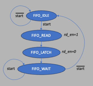
The last state machine will be the one to control the FIFO reading. This is a pretty simple one, and you might ask why we don't just enclose it inside the RX FSM that we just made. We could do that, but making it separate allows us to extend functionality in subsequent projects!
The FSM diagram is shown next:
    //
    //  this FSM controlls the FIFO reading
    //
    localparam [1:0] FIFO_IDLE=0, FIFO_READ=1, FIFO_LATCH=2, FIFO_WAIT_DONE=3;
    reg [1:0] f_state;
    reg [15:0] f_data_out;
    reg [16:0] f_count_out;
    reg f_rd_en;
    reg f_done;
    wire fifo_last = (fifo_data_count == 10'h1);
    wire [3:0] bottom_bits = {1'b0,fifo_full,fifo_empty,fifo_last};
    always @ (posedge clock25)
        if (reset) begin
            f_state <= FIFO_IDLE;
            f_data_out <= 0;
            f_count_out <= 0;
            f_done <= 0;
            f_rd_en <= 0;
        end
        else case (f_state)
            FIFO_IDLE: begin
                f_data_out <= 0;
                f_count_out <= 0;
                f_done <= 0;
                f_rd_en <= 0;
                if (fifo_rd) f_state <= FIFO_READ;
                else f_state <= FIFO_IDLE;
            end
            FIFO_READ: begin
                f_rd_en <= 1;
                f_state <= FIFO_LATCH;
            end
            FIFO_LATCH: begin
                f_rd_en <= 0;
                f_data_out <= {dout[15:4], bottom_bits[3:0]};
                f_count_out <= {6'h0,fifo_data_count[9:0]};
                f_state <= FIFO_WAIT_DONE;
            end
            FIFO_WAIT_DONE: begin
                f_done <= 1;
                if (fifo_rd) f_state <= FIFO_WAIT_DONE;
                else f_state <= FIFO_IDLE;
            end
        endcase
    assign rd_en = f_rd_en;
    assign fifo_data_latched = f_data_out;
    assign fifo_count_latched = f_count_out;
    assign fifo_done = f_done;
Finally, we want to drive the led signals, and the JB and JA PMOD blocks for debugging. For the led, let's use them to show what's going on:
assign led = {6'b0,rx_state[3:0],tx_state[2:0],fifo_empty,fifo_full,sw[0]};
And to see the the output of JB and JA
we include some useful signals for the logic analyzer, controlled by toggling
the slide switches 15, 14, and 13:
    always @ (*)
        case (sw[15:13])
            3'b000: begin
                JB = {rd_en,tx_done,tx,do_transmit,send_fifo_data,rx,clock25,clock1};
                JA = {f_rd_en,f_state[1:0],fifo_rd,rx_state[3:0]};
            end
            3'b001: begin
                JB = {adc_ready,adc_data_ready,isbusy,eos_out,adc_data[3:0]};
                JA = {rd_en,dout[6:0]};
            end
            3'b010: begin
                JB = received_byte[7:0];
                JA = {f_rd_en,f_state[1:0],fifo_rd,rx_state[3:0]};
            end
            3'b011: begin
                JB = {dv,rx_data[6:0]};
                JA = {f_rd_en,f_state[1:0],fifo_rd,rx_state[3:0]};
            end
            3'b100: begin
                JB = rx_data[7:0];
                JA = received_byte[7:0];
            end
            default: begin
                JB = {rd_en,tx_done,tx,do_transmit,send_fifo_data,rx,clock25,clock1};
                JA = {f_rd_en,f_state[1:0],fifo_rd,rx_state[3:0]};
            end
        endcase
The above project archive can be found here.
The code here will be similar to the previous Python tkinter programs. We will have a button to read the firmware version, the slide switches, a single ADC value from the fifo, and all of the data from the fifo. It's pretty easy to write tkinter code once you get the hang of it, and you can also draw things onto a "canvas" so in this code we will draw the voltmeter when we click on the single fifo read, and we will draw a plot of fifo data vs time (same as the fifo index).
First, import necessary libraries and start the Tk constructor:
from tkinter import *
import serial
import serial.tools.list_ports
import math
import time

root = Tk()
Next, set up the Application object, so that we can invoke buttons, text and label widgets, etc. What tkinter does is to take all of the widgets you define, which includes the row and column number (rows start 0 at the top and increase downward) and packs them so that they fit a table. So if you define 2 things in row 0 and 2 in row 1, it will figure out which has the biggest column width and make everything in the column fit that. Sometimes that can look awkward, so what we will do is to define something called a frame, and pack the frames in the TK root window, and pack the widgets into each frame. tkinter won't align the columns from frame to frame, only within the frame. So the next bit of code establishes the constructor for our Application class, the frames, and a few variables. The self.x syntax is the way python wants you to initialize variables within a class. Note that at the end we call "self.create_widgets()" to make all the widgets, but we could also have just put all the widget creation code inside this constructor. "openPort" is called to open a connection to the RPi serial port through the driver that comes in when you import serial. The line "self.voltages = []" creates an empty array.
class Application(Frame):
    """ Create the window and populate with widgets """

    def __init__(self,parent):
        """ initializes the frame """
        Frame.__init__(self,parent,background="white")

        self.frame1 = Frame(parent)
        self.frame1.grid(row=0,column=0,sticky=W)
        self.frame1.config(highlightthickness=1,highlightbackground="black")

        self.frame2 = Frame(parent)
        self.frame2.grid(row=1,column=0,sticky=W)
        self.frame2.config(highlightthickness=1,highlightbackground="black")

        self.debugit = False
        self.parent = parent
        self.canvas_width = 500
        self.canvas_height = 500
        self.grid()
        self.create_widgets()
        self.isopen = 0
        self.openPort()
        self.voltages = []
Next we create a function called "create_widgets" that instantiates the widgets we
need, associates them with a frame, and specifies the row/column within the frame.
Things like "Button", "Label", "Text", are all from the tkinter library. Note that
for the buttons, which will call functions when pushed, we use the python "lambda"
syntax when we want to pass arguments. Each of those functions has to be defined,
see below.
    def create_widgets(self):

        self.buttonQ = Button(self.frame1, text="Quit")
        self.buttonQ["command"] = self.quitit
        self.buttonQ.grid(row=0,column=0, sticky=W)

        self.fetchlabel = Label(self.frame1, text="Fetch:")
        self.fetchlabel.grid(row=0, column=1, sticky=W)

        #
        # set up the fetch buttons to send the address as an argument
        #
        self.buttonV = Button(self.frame1,text="Version")
        self.buttonV.grid(row=0,column=2, sticky=W)
        self.buttonV["command"] = lambda: self.getdata(7)

        self.buttonS = Button(self.frame1,text="Test")
        self.buttonS.grid(row=0,column=3, sticky=W)
        self.buttonS["command"] = lambda: self.getdata(5)

        self.buttonD = Button(self.frame1,text="Data")
        self.buttonD.grid(row=0,column=4, sticky=W)
        self.buttonD["command"] = lambda: self.getdata(3)

        self.buttonF = Button(self.frame1,text="Fifo Once")
        self.buttonF.grid(row=0,column=4, sticky=W)
        self.buttonF["command"] = lambda: self.getdata(1)

        self.buttonF = Button(self.frame1,text="Fifo All")
        self.buttonF.grid(row=0,column=5, sticky=W)
        self.buttonF["command"] = lambda: self.getalldata()

        self.buttonDC = Button(self.frame1,text="Fifo Count")
        self.buttonDC.grid(row=0,column=6, sticky=W)
        self.buttonDC["command"] = lambda: self.getdata(9)

        self.slabel = Label(self.frame2, text="Status:")
        self.slabel.grid(row=0, column=0, sticky=W)

        self.status = Text(self.frame2,height=1,width=40)
        self.status.grid(row=0, column=1, columnspan=4, sticky=W)
        self.status.delete("1.0",END)

        self.rlabel = Label(self.frame2, text="Result:")
        self.rlabel.grid(row=1, column=0, sticky=W)

        self.answer = Text(self.frame2,height=1, width=40)
        self.answer.grid(row=1,column=1,columnspan=4, sticky=W)
        self.answer.delete("1.0",END)

        self.C = Canvas(self,bg="white",height=self.canvas_height,width=self.canvas_width)
        self.C.grid(row=2,column=0,columnspan=5)
Next we define the functions we need. "quitit" is a general purpose function
to quit, just for fun. The "getdata16" function is a good one to look at to learn
how to send and receive bytes from the BASYS3. In "getdata16", we first
we first check that the port is opened ok. Then we want to send the "address",
which is just the data byte that the FPGA will use to figure out what to send
back. The line
    def quitit(self):
        print("That's all folks!")
        quit()

    def openPort(self):
        if self.isopen == 1:
            self.status.insert(END,"Port is already open!\n")
            self.ser.close()
            return
        #
        #   defaults
        #
        port = "/dev/ttyS0"
        sbaud = "1000000"
        baud = int(sbaud)
        timeout = 2
        if self.debugit: print("port="+port+"  baud="+sbaud)
        self.ser = serial.Serial(port,sbaud,timeout=timeout)
        if self.ser.isOpen():
            self.status.insert(END,self.ser.name + " is now open\n")
            if self.debugit: print(self.ser.name + " is now open...")
            self.isopen = 1
        else:
            self.status.insert(END,self.ser.name + " is NOT open!!!\n")
            if self.debugit: print("sorry, problem trying to open port "+port+"\n")

    def getalldata(self):
        if self.debugit:
            print("getalldata:")
            print("reading fifo 1024 times....")
        self.voltages.clear()
        for n in range(0,1024):
            idata = self.getfifodata(1)
            if idata < 0:
                break
            last = idata & 1
            empty = (idata >> 1) & 1
            full = (idata >> 2) & 1
            val = idata >> 4
            voltage = val * 0.244E-3
            self.voltages.append(voltage)
            if self.debugit: print("  voltage: ",str(voltage)+" full "+str(full)+" empty "+str(empty)
                +" last "+str(last))
            self.answer.delete(1.0,END)
            self.answer.insert(1.0,hex(idata) + " = " + str(voltage)+" volts")
            if empty or last:
                break
        print("Read "+str(n)+" words from the FIFO")
        self.answer.delete(1.0,END)
        self.answer.insert(1.0,"Read "+str(n)+" words from the FIFO")
        print("making plot...")
        self.plot()
        print("done!")

    def getdata(self,addr):
        if self.debugit: print("getdata:")
        idata = self.getfifodata(addr)
        if idata < 0:
            return
        if self.debugit: print("  value read in hex: "+hex(idata))
        self.status.delete(1.0,END)
        self.status.insert(1.0," Success!!!")
        self.answer.delete(1.0,END)
        if addr == 3 or addr == 1:
            val = idata >> 4
            if self.debugit: print("  12 bit value: ",hex(val))
            #
            #   now calculate the votage read
            #
            voltage = val * 0.244E-3
            if self.debugit: print("  voltage: ",str(voltage))
            self.answer.delete(1.0,END)
            self.answer.insert(1.0,hex(idata) + " = " + str(voltage)+" volts")
            self.display(voltage)
        if addr == 9:
            if self.debugit: print("  value received: ",hex(idata))
            self.answer.delete(1.0,END)
            self.answer.insert(1.0," fifo count = " + str(idata))
        if addr == 5 or addr == 7:
            self.answer.insert(1.0,hex(idata))

    def getfifodata(self,addr):
        if self.debugit: print("getfifodata:")
        #
        # check to see if any port has been opened or not
        #
        if self.isopen == 0:
            print("  you must open a port first!!!")
            self.status.delete(1.0,END)
            self.status.insert(1.0,"Sorry but you MUST open a port first!")
            return -1
        #
        # fetch what?
        #
        if addr == 0:
            print("  invalid address "+str(addr))
            self.status.delete(1.0,END)
            self.status.insert(1.0,"??? invalid address!!!")
            return -1
        #
        # send the command
        #
        if self.debugit: print("  sending "+str(addr))
        self.status.delete(1.0,END)
        self.status.insert(1.0,"Sending...")
        sendb = addr.to_bytes(1,"little")
        self.ser.write(sendb)
        self.status.insert(END,"done!")
        #
        # now read the data transmitted from the FPGA to the RPi
        #
        nbytes = 2
        self.status.insert(END,"  Waiting...")
        tdata = self.ser.read(nbytes)
        if len(tdata) == 0:
            print("  length 0, must be a timeout!!!")
            self.status.delete(1.0,END)
            self.status.insert(1.0,"Timeout!!!")
            return -1
        idata = int.from_bytes(tdata,byteorder="little")
        return idata
The next few subroutines are for displaying graphics on the canvas that
we created above with the line
    def display(self,volts):
        self.C.delete("all")
        #
        #   draw a circle centered at half the canvas width and height
        #   with radius circle_radius
        #
        circle_radius = 100
        circle_center_x = self.canvas_width/2
        circle_center_y = circle_radius + 50
        print(str(circle_radius))
        print(str(circle_center_x))
        print(str(circle_center_y))
        left_x = circle_center_x - 100
        right_x = circle_center_x + 100
        left_y = circle_center_y - 100
        right_y = circle_center_y + 100
        self.C.create_oval(left_x,left_y,right_x,right_y)
        #
        #   voltage goes from 0 to 1, so scale the angle of
        #   the meter line
        #
        angle = math.pi * volts
        linex = circle_radius * math.cos(angle)
        liney = circle_radius * math.sin(angle)
        x0 = circle_center_x
        y0 = circle_center_y
        self.C.create_line(x0,y0,x0-linex,y0-liney)
        for i in range(0,11):
            val = float(i)/10
            sval = str(val)
            ang = math.pi * val
            x1 = x0 - (circle_radius+10) * math.cos(ang)
            y1 = y0 - (circle_radius+10) * math.sin(ang)
            self.C.create_text(x1,y1,text=sval)

    def plot(self):
        self.C.delete("all")
        xoff = 50
        yoff = 50
        voltmax = 1.0
        nmax = len(self.voltages)
        if nmax == 0:
            print("  no data to plot!")
            return
        width = self.canvas_width
        height = self.canvas_height
        pw = width - 2*xoff
        ph = height - 2*yoff
        self.C.create_rectangle(xoff,yoff,width-xoff,height-yoff)
        n = 0
        radius = 1
        xold = 0
        yold = 0
        #
        #   display the y axis, voltage
        #
        self.C.create_text(xoff-20,20,text="Voltage")
        self.C.create_text(xoff-15,height-yoff,text="0.0")
        self.C.create_text(xoff-15,height-yoff-0.25*ph,text="0.25")
        self.C.create_text(xoff-15,height-yoff-0.5*ph,text="0.5")
        self.C.create_text(xoff-15,height-yoff-0.75*ph,text="0.75")
        self.C.create_text(xoff-15,height-yoff-ph,text="1.0")
        for volt in self.voltages:
            y = height - yoff - volt*ph/voltmax
            x = xoff + n*pw/nmax
            x0 = x - radius
            x1 = x + radius
            y0 = y - radius
            y1 = y + radius
            self.C.create_oval(x0,y0,x1,y1)
            if n == 0:
                xold = x
                yold = y
            else:
#               self.C.create_line(x,y,xold,yold)
                xold = x
                yold = y
            n += 1
        if self.debugit: print("  done!")


def main():

    # modify the window
    root.title("Python/BASYS3 Voltclockfifo - RPi control")
    root.wm_title("Python/BASYS3 Voltclockfifo - RPi control")
    root.geometry("500x600+500+200")
    root.update()

    #create the frame that holds other widgets
    app = Application(root)

    #kick off event loop
    root.mainloop()


if __name__ == '__main__':
    main()
To run the FPGA, make sure that the bottom slide switch is set to off (down) when you load the program so that it doesn't start entering anything into the fifo yet. Then hit the reset button and make sure everything is in the right state. The bottom LED will be on when sw[0] is on, the next led is the fifo_full flag, and, the next one is fifo_empty. In the initial state, you should see only led[2] (3rd from the right) on. Then if you toggle the switch on and then off, you should see the fifo_empty led go off and the fifo_full line go on right away. Remember we are running the FIFO at 1MHz and it is only 1024 deep so it will get full in 1ms. Then, run the "voltclockfifo.py" code and you can read 16 bits data words from the BASYS3.
I ran with a voltage source that puts out 0 to 1 volt into the JXADC PMOD port, and configured the source so that I had a push button. After several attempts I was able to turn on the FIFO write (sw[0]) fast enough to catch the transition from 0 to 0.5 volts in the FIFO and read it out by clicking the "Fifo All" button:
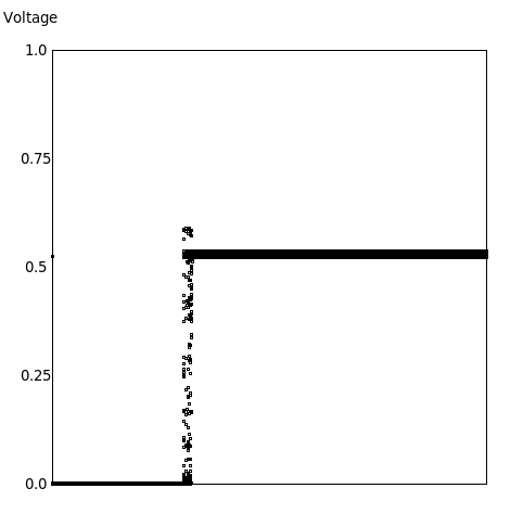
You can see the nice edge. And, you can see the bouncing, and how the bouncing must be producing some kind of inductance overshooting.
I also looked at the signals on the logic analyzer and captured this:
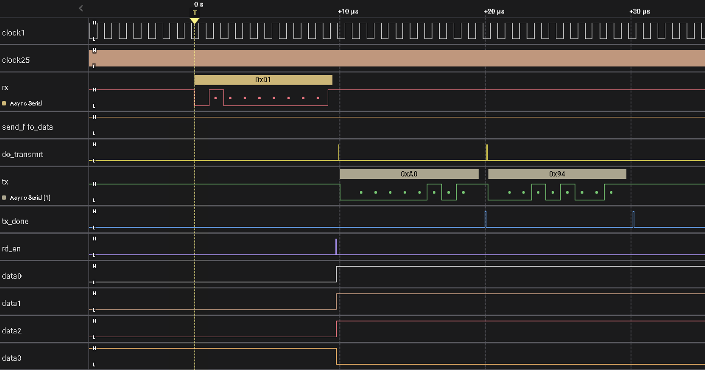
The logic analyzer (SALEAE) can look at a line as if it was a serial UART line and decode it and display the value about it. In the figure above, yo usee the 1MHz clock line on the top followed by the 25MHz clock that runs the UART and FSMs. The 3rd line is the "rx" line, from the FPGA, so that's the line that goes low when the RPi wants to send data. It is sending a 0x1 byte, and that code means send back a single 16 bit read from the fifo. The FSM then asserts do_transmit twice, one for each byte, and sends back 0xA0 followed by 0x96, and since we are using "little endian", the RPi will see that as 0x94a0 (first byte is low, 2nd is high). You can see the tx_done line go high for each transmission, and the rd_en go high before the transmissions which means that the FIFO was read and then data sent out. The lines "data0", "data1", "data2" are just a few of the lower order bits of the FIFO data to show that the lines are transitioning synchronous with rd_en, which is what you expect.
This documentation goes with the Vivado project "voltclockfifo".