In all of the previous labs, we are running the serial connection at 1Mbaud. That means that each bit has a 1μs width. For UART connections, we use 1 start bit and 1 stop bit, with 8 bits in between, for a total of 10, which means that it takes 10μs to send 1 byte, or 100kBps. As shown in the Digital Oscilloscope lab, due to the overhead in the RPi, we are able to send 1 byte every 450μs, or 2.2kBps, which is a pretty low efficiency. This is due to the fact that our protocols require the RPi to send a message to the FPGA each time it wants another byte sent. So in this lab, we will try to boost the data rate from the FPGA to the RPi by simplifying the protocol in the RPi, but increasing the complexity in the FPGA.
What we will do is to introduce a "blast" mode, where the FPGA just sends bytes as fast as it can. Note that in the RPi, to receive data we would execute a serial.read(n) command where n is the number of bytes. The RPi would then collect those bytes and put them into a byte array, so the only overhead there is due to what goes on inside the pyserial library for reading. This means that we have to have an agreement between the number of bytes sent to the RPi and the number of bytes the RPi will wait for.
Let's make a new project and call it "blast", and a top level top.v module. The module will have pretty much all of the usual inputs and outputs as in the previous project Digital Oscilloscope:
module top(
    input clock,            // system clock
    input reset,            // BTNR
    input version,          // BTNU
    input adc_n, adc_p,     // VCAUX 6, P and N
    input [15:0] sw,        // slide switches
    output [15:0] led,      // 16  onboard LEDs above the switches
    output [6:0] segment,   // 4 digit LED display
    output dp,              // "." next to each LED digit
    output [3:0] digit,     // which of 4 7-segment digits
    output reg [7:0] JB,    // debugging
    output reg [7:0] JA,    // debugging
    input rx,               // UART receive
    output tx               // UART transmit
    );
    parameter VERSION = 'h2001;
Next lets make the 25MHz clock for the uart receive and transmitter (and state machines that control them). In the Clocking Wizard, use the "Component Name" clock25 and set the output clk_out1 to 25.000.
    //
    //  a 25MHz clock for the uart rx and tx, and the state machines that control them
    //
    wire locked, clock25;
    clock25 MYCLOCK25 (
        .reset(reset),
        .clk_in1(clock),
        .locked(locked),
        .clk_out1(clock25)
    );
Next we have to make clocks for the XADC digitizing, and the ADC FIFO to store the data. In anticipation of the next project (audio), let's make the XADC digitize at a standard 44.1kHz audio rate, which means that we will want to write data into the ADC FIFO at that same rate in order to keep up.
XADC DCLK
As described in the Using the FPGA ADC lab, the XADC module takes the DCLK input and divides it by some clock divider value and then divides by 26 (since it needs 26 clocks per conversion) to get the ADC Conversion Rate. Using the audio rate of 44.1kHz and multiplying by 26 gives 1.1466MHz. To get over the DCLK minimum of 8MHz we can use a clock divider of 8 inside the XADC module, which means we need to generate an XADC input clock that is 8×1.1466=9.1728MHz. We can generate this new clock using the Clocking Wizard in the IP Catalog, but if you try this you will find that due to the numerology of how the FPGA generates clocks, the closest clock it can get to 9.1728MHz is 9.17281MHz, which corresponds to an audio conversion rate of 44.10005kHz instead of 44.1kHz. This is probably good enough, however we can get it pretty much exact by first generating a 101MHz clock (using the 100MHz system clock), and then using the 101MHz clock to generate the 9.1728MHz clock that goes into the XADC. So we will need to generate 2 more clocks: 101MHz using the 100MHz system clock, and 9.1728MHz using the 101MHz generated clock. Let's call these clocks clock101 and xadc_clock respectively in the verilog, and generate them using 2 different instantiations of the Clocking Wizard, where in the first one, clock101 will have clk_in1 equal to 100MHz and clk_out1 at 101MHz, and in the second, xadc_clock will have clk_in1 equal to 101MHz and clk_out1 at 9.1728MHz.
After making these new modules with the Clocking Wizard, the instantiation looks like this, where the clock signal xadc_clock is what will be input to the XADC block below.
    //
    //  for the XADC DCLK clock, we want a clock that is an even multiple of 2 times
    //  the 44.1kHz samping rate times 26, since there are 26 clocks per sample.
    //  so 44.1kHz x 26 = 1146.6kHz.  The XADC minimum is 8000kHz, so if we use
    //  8 x 1146.6 = 9.1728Mhz, we will get a 44.1kHz sampling.
    //
    //  turns out that we first have to generate a 101MHz clock, then use that to
    //  generate the 9.1728MHz clock
    //
    wire locked101, clock101;
    clock101 CLOCK101 (
        .reset(reset),
        .clk_in1(clock),
        .locked(locked101),
        .clk_out1(clock101)
    );
    wire locked3, xadc_clock;
    clock_xadc XADC_CLOCK (
        .reset(reset),
        .clk_in1(clock101),
        .locked(locked3),
        .clk_out1(xadc_clock)
    );
ADC FIFO write clock
For the FIFO write clock, we want to generate a 44.1kHz clock. Given the 8MHz minimum of the Clocking Wizard, we can use it to generate a clock that is 44.1kHz×2N>8MHz, which is solved by setting N = 8, which gives us a clock of 44.1kHz×256=11.2896MHz. Then we can make an 8 bit counter that is incremented using the 11.2896MHz clock, and put the MSB through a clock buffer to get the nice clean 44.1kHz write clock for the ADC FIFO. So in the CLocking Wizard, let's call the "Component Name" adc_fifo_clock and set the clk_out1 to 11.2896. The code instantiation will be:
    //
    //  we want the XADC to deliver an audio signal at 44.1kHz.   The minimum output
    //  clock is 8MHz, so we need the lowest multiple of 44.1kHz in powers of 2 that
    //  generates a clock with f>8MHz, which is 256x0.0441=11.2896MHz
    //
    //  for the FIFO clock, we want 44.1kHz so if we generate a 11.2896 MHz clock
    //  and divide it down by 256 using an 8 bit counter using the MSB, we will get
    //  the 44.1kHz FIFO write clock
    //
    wire locked2, clock256;         // will be 256 times the FIFO clock
    adc_fifo_clock ADC_CLOCK (
        .reset(reset),
        .clk_in1(clock),
        .locked(locked2),
        .clk_out1(clock256)
    );
    wire fifo_clock;            // will be 44.1kHz
    reg [7:0] count1;
    always @ (posedge clock256)
        if (reset) count1 <= 0;
        else count1 <= count1 + 1;
    BUFG fifoclock (.I(count1[7]), .O(fifo_clock));
Next, instantiate the 7-segment display:
    //
    //  next drive the 4 7-segment displays
    //
    wire [15:0] display_this;
    display4 DISPLAY (
        .clk100(clock),
        .number(display_this),
        .digit(digit),
        .segments(segment),
        .period(dp)
        );
Next, we need to make an XADC module using the IP Catalog. Let's call the component name myxadc and use xadc_clock as the input clock, and set the ADC Conversion Rate to 44.1kHz. The module will calculate it's clock divider and it should come out to be 8. As detailed in the Using the FPGA ADC lab, we will latch the data out of the XADC with the negedge of the isbusy signal. We will also make a roughly 1 Hz clock and latch the value latched out of the XADC to put onto the 7-segment display.
The instantiation looks like this:
    //
    //  here is the XADC block
    //
    wire [6:0] daddr_in = 7'h16;
    wire adc_ready, isbusy, adc_data_ready, eos_out, alarm;
    wire [15:0] adc_data;
    wire [4:0] channel_out;
    myxadc XADC_INST (
        .daddr_in(7'h16),   // specifies vcaux6 pints to digitize
        .dclk_in(xadc_clock),    // 9.1728MHz clock
        .den_in(adc_ready), // tied to adc_ready, tells adc to convert, tieing causes continuous conversions
        .di_in(16'h0),      // to set the data to something, not used here
        .dwe_in(1'b0),      //  set to enable writing to di_in, which we don't want to do
        .vauxp6(adc_p),     //  positive input to digitize
        .vauxn6(adc_n),     //  negative input to digitize
        .busy_out(isbusy),  // tells you the adc is busy converting
        .channel_out(channel_out[4:0]), // for using more than 1 channel, tells you which one.  not used here
        .do_out(adc_data),      // adc value from conversion
        .drdy_out(adc_data_ready),  //tells you valid data is ready to be latched
        .eoc_out(adc_ready),   //  specifies that the ADC is ready (conversion complete)
        .eos_out(eos_out),     //  specifies that conversion sequence is complete
        .alarm_out(alarm),      // OR's output of all internal alarms, not used here
        .vp_in(1'b0),           // dedicated analog input pair for differential, tied to 0 if not used
        .vn_in(1'b0)
    );
    //
    // wait for XADC to tell you something is ready to latch. note this means continuous latching
    //
    reg [15:0] r_adc_data;
    always @ (negedge isbusy) begin
        if (reset) r_adc_data <= 16'h0;
        else r_adc_data <= adc_data;
        end
    //
    //  make a ~1Hz clock so we can run the LED display slower
    //
    reg [27:0] counter;
    reg [15:0] s_adc_data;
    always @ (posedge clock) begin
        if (reset) counter <= 0;
        else counter <= counter + 1;
        end
    wire clock_1hz = counter[27];
    always @ (posedge clock_1hz) s_adc_data <= r_adc_data;
    assign display_this = version ? VERSION : s_adc_data;
Now let's make the ADC FIFO using the IP Catalog and call it "fifo_adc" in the "Components Name" field. We will make it 18 bits wide and 16 bits of addresses deep, which means the FIFO will hold 65536 data points. We also will enable "Read Data Count" in the "Data Counts" tab so that we can know how many data points are left to be read. Note that if each data point is taken at 44.1kHz, then the full FIFO represents a total time of 65531/44.1kHz = 1.49 seconds worth of data. That should be plenty in order to do fourier analysis, but you can increase it later if you like (however remember that the data count will also have to change.)
We will use the fifo_clock as the write clock, and read it with the faster 25MHz clock so that we can blast data out to the RPi. The input to the FIFO is just the 16 bits of ADC data latched into r_adc_data with an extra 2 bits set to 0 to make 18 bits. We will also use led[2] to indicate that there is only 1 word left in the FIFO, led[3] set to fifo_empty, and led[4] set to fifo_full.
    //
    //  now instantiate the ADC FIFO.  the write clock will be the fifo_clock (44.1kHz) but the
    //  read clock will be 25MHz because we want to blast data out as soon as the fifo is full
    //  and we get a request from the RPi
    //
    wire [17:0] din = {2'b00,r_adc_data};   // feed this directly into the FIFO data input
    wire [17:0] dout;
    wire [11:0] fifo_adc_out = dout[15:4];  // only keep the 12 bits of ADC data
    wire wr_en;
    wire rd_en, fifo_full, fifo_empty, wr_rst_busy, rd_rst_busy;
    wire [15:0] fifo_data_count;
    fifo_adc DATA_FIFO (
        .rst(reset),
        .wr_clk(fifo_clock),
        .rd_clk(clock25),
        .din(din),
        .wr_en(wr_en),
        .rd_en(rd_en),
        .dout(dout),
        .full(fifo_full),
        .empty(fifo_empty),
        .rd_data_count(fifo_data_count),
        .wr_rst_busy(wr_rst_busy),
        .rd_rst_busy(rd_rst_busy)
    );
Next, the uart rx and tx modules, and the uart rx FIFO module to FIFO incoming
commands from the RPi. Since the incoming data is 8 bits, we can make the rx FIFO
8 bits wide and we don't need a large depth so have the "Write Depth" be 16, that
will be plenty since the RPi is only sending a byte at a time.
To generate the rx FIFO, use the name "rxfifo", with
independent BRAM clocks, and no need to generate the read data count.
    //
    //  instantiate the UART receiver.  run with the 25MHz clock so that
    //  we can stay in phase with the state machines that control things
    //
    wire dv;
    wire [7:0] rx_data;
    uart_rx RECEIVER (
        .i_Clocks_per_Bit('d25),
        .i_Clock(clock25),
        .i_Reset(reset),
        .i_Rx_Serial(rx),       // tied to FPGA rx output
        .o_Rx_DV(dv),
        .o_Rx_Byte(rx_data)
        );
    //
    //  instantiate a fifo for the UART receiving from the RPi
    //  tie rx_wr_en to dv so that we can have the fifo write clock
    //  always going.  use the same for the read clock
    //
    wire rx_wr_en = dv;
    wire rx_full, rx_empty;
    wire rx_rd_en;
    wire [7:0] rx_dout;
    rxfifo FIFO_RX  (           // this fifo is 9 bits wide
        .rst(reset),
        .wr_clk(clock25),
        .rd_clk(clock25),
        .din(rx_data),
        .wr_en(rx_wr_en),
        .rd_en(rx_rd_en),
        .dout(rx_dout),         // and 9 bits out
        .full(rx_full),
        .empty(rx_empty)
    );
    //
    //  instantiate the UART transmitter
    //
    wire tx_active, tx_done;
    wire do_transmit;
    wire [7:0] transmit_byte;
    uart_tx TRANSMITTER (
        .i_Clocks_per_Bit('d25),
        .i_Clock(clock25),
        .i_Reset(reset),
        .i_Tx_DV(do_transmit),
        .i_Tx_Byte(transmit_byte),
        .o_Tx_Active(tx_active),
        .o_Tx_Serial(tx),       // tied to FPGA tx output
        .o_Tx_Done(tx_done)
        );
Note that we will assign led[0] to be the uart rx FIFO empty signal, and led[1] to be the FIFO full signal (see below).
Next we implement the same state machine as in previous projects to control sending out 2 bytes at a time:
    //
    //  now make a state machine to deal with transmitting 2 bytes at a
    //  time, including the FIFO value that is present.
    //
    reg [2:0] tx_state;     // 8 states so 3 bits will do
    localparam [2:0] TX_IDLE=0, TX_BYTE1=1, TX_DO1=2, TX_WAIT1=3,
        TX_BYTE2=4, TX_DO2=5, TX_WAIT2=6, TX_DONE=7;
    reg doit;
    wire [15:0] transmit_word;
    wire begin_transfer;
    reg [7:0] tx_data;
    always @ (posedge clock25) begin
        if (reset) begin
            tx_state <= TX_IDLE;
            doit <= 0;
            tx_data <= 0;
        end
        else
            case (tx_state)
                TX_IDLE: begin
                    //
                    //  wait for begin_transfer to start
                    //
                    if (begin_transfer) tx_state <= TX_BYTE1;
                    else tx_state <= TX_IDLE;
                    doit <= 0;
                    tx_data <= 0;
                end
                TX_BYTE1: begin
                    //
                    //  latch the first byte of the transmit_word
                    //
                    tx_data <= transmit_word[7:0];
                    tx_state <= TX_DO1;
                end
                TX_DO1: begin
                    //
                    //  turn on uart_tx
                    //
                    doit <= 1;
                    tx_state <= TX_WAIT1;
                end
                TX_WAIT1: begin
                    //
                    //  turn off doit and wait for uart_tx to finish
                    //
                    doit <= 0;
                    if (tx_done) tx_state <= TX_BYTE2;
                    else tx_state <= TX_WAIT1;
                end
                TX_BYTE2: begin
                    //
                    //  latch the 2nd byte to transfer
                    //
                    tx_data <= transmit_word[15:8];
                    tx_state <= TX_DO2;
                end
                TX_DO2: begin
                    //
                    //  turn on uart_tx
                    //
                    doit <= 1;
                    tx_state <= TX_WAIT2;
                end
                TX_WAIT2: begin
                    //
                    //  wait for the 2nd byte to finish begin sent
                    //
                    doit <= 0;
                    if (tx_done) tx_state <= TX_DONE;
                    else tx_state <= TX_WAIT2;
                end
                TX_DONE: begin
                    //
                    //  wait for begin_transfer to go away
                    //
                    if (do_transmit) tx_state <= TX_DONE;
                    else tx_state <= TX_IDLE;
                end
                default: begin
                    tx_state <= TX_IDLE;
                end
            endcase
    end
    assign do_transmit = doit;
    assign transmit_byte = tx_data;
Now we need to make a controller that will respond to RPi commands. We can use a controller similar to what we built in the previous >Digital Oscilloscope project, but we won't need a threshold or prefill register. However, as we showed in that project towards the end, the transfer speed was only around 450μs per each 2 byte transfer, and this time was entirely due to the RPi executing the code that first sends a byte to tell the FPGA what to transfer, then getting ready for the transfer. If instead we had the RPi send a byte telling the FPGA to send more than just 2 bytes, we might be able to blast much more data to the RPi. So let's build a controller that is similar to the one used in the >Digital Oscilloscope project that can:
`timescale 1ns / 1ps
//////////////////////////////////////////////////////////////////////////////////
//
//  this module assumes that in the level above, there's a FIFO that buffers all
//  UART receive transmissions.
//
//  the rx_data contains the relevant data to decode:
//
//  7654 3210
//              LSB=1 means the RPi is sending info that will come on the next transmission
//              All transactions are 8 bits
//  0000 0001   RPi is sending control register (on/off...etc)
//  0000 0011   "    "   "     blast register
//
//              LSB=0 means RPi wants FPGA to send stuff back
//  0000 0010   send back 16 bit ADC value from XADC block directly
//  0000 0100   send back 16 bit test value from slide switches
//  0000 0110   send back 16 bit firmware version
//  0000 1000   send back 8 bit control register (upper 8 bits are all zero)
//  0000 1010   send back 8 bit status register (ditto)
//  0000 1100   semd back 16 bit blast register
//  0000 1110   send back the ADC data fifo counts
//  1000 0000   blast back 65536 data points from ADC fifo or until empty
//
module controller(
    input clock25,              // 25MHz input clock to match uart_rx and uart_tx clock and adc fifo read
    input fifo_clock,           // fifo input clock, which should be 44.1kHz
    input reset,                // reset (BTNR)
    output global_start,        // drive one of the LEDs with this line
    //
    //  rx fifo stuff
    //
    input rx_fifo_empty,        // fifo empty
    input [7:0] rx_fifo_data,   // 8 bits of fifo data
    output rx_fifo_rd_en,       // fifo read enable
    //
    //  uart_tx stuff
    //
    output [15:0] tx_transmit_out,      //  2 bytes to send out
    output tx_transmit,                 //  signal to send them
    input tx_done,                      //  asserted twice per transfer
    //
    //  data inputs
    //
    input [15:0] version,           //  set at the top of top.v
    input [15:0] test,              //  slide switches
    input [15:0] adc_data,          //  latched into r_adc_data
    //
    //  ADC fifo stuff
    //
    input adc_fifo_empty,                   //  fifo empty
    input adc_fifo_full,                    //  fifo full
    output reg adc_fifo_rd,                 //  read enable
    output adc_fifo_wr,                     //  write enable
    input [15:0] adc_fifo_data_count,       //  number left to read
    input [15:0] adc_fifo_data,             //  all 16 bits of data
    //
    //  debug
    //
    output [49:0] debug
    );
First we define "blast", control, and status registers. blast will need to be 16 bits, so we might as well make control and status also 16 bits even though we might not need that many bits there (see below). This means that the state machine that sends data back to the RPi can be the same one as in the Digital Oscilloscope project.
For control, we will need one bit for a global start, and perhaps another bit to facilitate testing. For instance, we can have a test mode where instead of the FPGA sending data from the FIFO, it can send a counter so that in the RPi, we can make sure that we are getting the right amount of consecutive data. Note that the way the RPi serial input works is that all of the data is received and buffered, then you read some number of bytes at a time using software. On the RPi, the serial input buffer is 4096 bytes deep. In principle this could be changed but you probably would have to recompile the pyserial libraries. So for this lab, we will use the 4096 limit, which means we only want to read the FIFO (which has 16 bits = 2 byte words) 2048 times. So when we start reading in the BLAST state machine we start at 0 and read the FIFO until the counter gets to 2047 = 0x7FF. So we set the blast register initially to 0x7FF.
For the 16 bits of status register, let's have the LSB be global_start, then a 0, then rx_fifo_empty, adc_fifo_empty, adc_fifo_full, followed by 11 0's. The 1st 0 is to make the software compatible with previous projects.
The instantiation should be:
    //
    //  "blast" register tells how many data points from the ADC FIFO to send to the
    //  RPi in one continuous "blast"
    //
    //  note that the FIFO is 65535 deep, so we set the blast register to that value
    //  and the RPi will expect to receive 65536 x 2 bytes
    //
    reg [15:0] blast = 16'h7FF;
    //
    //  here is the control register, which might have only 1 bit for global start
    //
    reg [15:0] control;
    assign global_start = control[0];
    assign test_mode = control[1];
    //
    //  status register
    //
    wire [15:0] status = {11'b000,adc_fifo_full,adc_fifo_empty,rx_fifo_empty,1'b0,global_start};
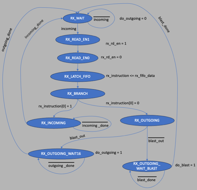
Next comes the state machine that handles incoming traffic from the RPi. We can use one that we built for the Digital Oscilloscope project, with some changes. In this version, we will separate "outgoing" tasks into those that consist of sending the 16 bit words internal to the firmware (version, test, and adc), and the blasting of data from the ADC FIFO. This is shown below. It looks a little complicated but mostly that's because the "OUTGOING" state has been split into the "RX_OUTGOING_WAIT16" (for the 16-bit values) and "RX_OUTGOING_WAIT_BLAST" for the ADC FIFO data.
The code is next:
    //
    //  here is the rx state machine, it looks at the rx fifo empty flag to know if it has
    //  anything to process
    //
    wire incoming = ~rx_fifo_empty;  // this is the signal that the fifo has something in it to process
    localparam [3:0] RX_WAIT=0, RX_READ_EN1=1, RX_READ_EN0=2,
        RX_LATCH_FIFO=3, RX_BRANCH=4, RX_INCOMING=5, RX_OUTGOING=6,
        RX_OUTGOING_WAIT16=7, RX_OUTGOING_WAIT_BLAST=8;
    reg [3:0] rx_state;
    reg [7:0] rx_instructions;
    reg do_read_fifo, do_incoming, do_outgoing, do_blast;
    wire read_fifo_done, incoming_done, outgoing_done, blast_done;
    wire branch_to_incoming = rx_instructions[0];       // incoming or outgoing
    wire blast_out = rx_instructions[7];
    always @ (posedge clock25)
        if (reset) begin
            rx_state <= RX_WAIT;
            do_read_fifo <= 0;
            do_incoming <= 0;
            do_outgoing <= 0;
            rx_instructions <= 0;
            do_blast <= 0;
        end
        else case (rx_state)
            RX_WAIT: begin
                rx_instructions <= 0;
                do_read_fifo <= 0;
                do_incoming <= 0;
                do_outgoing <= 0;
                do_blast <= 0;
                rx_state <= incoming ? RX_READ_EN1 : RX_WAIT;
            end
            RX_READ_EN1: begin
                do_read_fifo <= 1;
                rx_state <= RX_READ_EN0;
            end
            RX_READ_EN0: begin
                do_read_fifo <= 0;
                rx_state <= RX_LATCH_FIFO;
            end
            RX_LATCH_FIFO: begin
                rx_instructions <= rx_fifo_data;
                rx_state <= RX_BRANCH;
            end
            RX_BRANCH: begin
                rx_state <= branch_to_incoming ? RX_INCOMING : RX_OUTGOING;
            end
            RX_INCOMING: begin
                do_incoming <= 1;
                rx_state <= incoming_done ? RX_WAIT : RX_INCOMING;
            end
            RX_OUTGOING: begin
                //
                //  check if we are outputing things like version, test, or adc, vs
                //  blasting data from the adc fifo
                //
                if (blast_out) rx_state <= RX_OUTGOING_WAIT_BLAST;
                else rx_state <= RX_OUTGOING_WAIT16;
            end
            RX_OUTGOING_WAIT_BLAST: begin
                do_blast <= 1;
                rx_state <= blast_done ? RX_WAIT : RX_OUTGOING_WAIT_BLAST;
            end
            RX_OUTGOING_WAIT16: begin
                do_outgoing <= 1;
                rx_state <= outgoing_done ? RX_WAIT : RX_OUTGOING_WAIT16;
            end
            default: begin
                rx_state <= RX_WAIT;
            end
        endcase
The registers do_incoming, do_outgoing, and do_blast trigger the relevant FSMs that handle those conditions. Again, we will use a hard handshake where this RX FSM will enter either the "RX_INCOMING" or "RX_OUTGOING" state, assert the relative lines to get things going, and wait for a done signal from each. "Blasting" occurs when the LSB of the incoming byte from the RPI is set to 0, and the MSB is set to 1.
Next we need state machines that will process the incoming (RPi sending data to the FPGA) and outgoing (FPGA sending data to the RPi). Just like in the previous project, we will be sending 16 bit words so we can use the same FSM, so it will look like this:
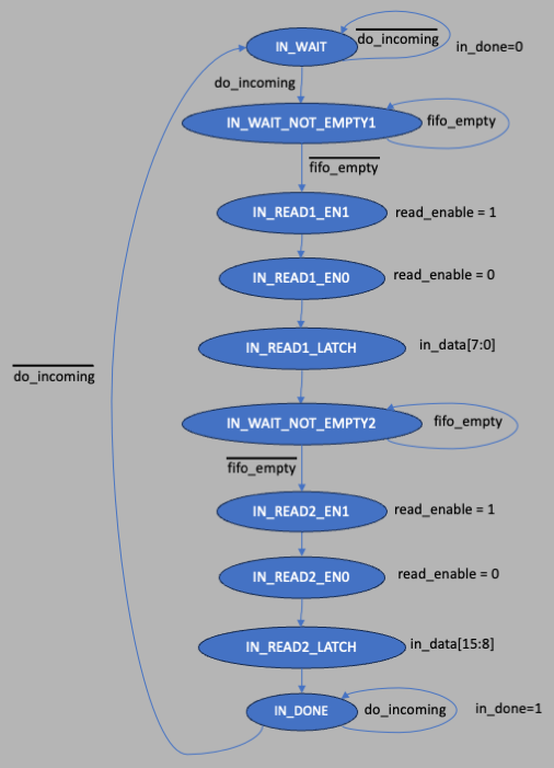
The code will be:
    //
    //  here is the "incoming" FSM that responds to the RPi sending data to the FPGA
    //
    localparam [3:0] IN_WAIT=0, IN_WAIT_NOT_EMPTY1=1, IN_READ1_EN1=2, IN_READ1_EN0=3, IN_READ1_LATCH=4,
        IN_WAIT_NOT_EMPTY2=5, IN_READ2_EN1=6, IN_READ2_EN0=7, IN_READ2_LATCH=8, IN_DONE=9;
    reg [3:0] in_state;
    reg in_read_fifo;
    reg in_done;
    reg [15:0] in_data;
    reg incoming_what;
    always @ (posedge clock25)
        if (reset) begin
            in_state <= IN_WAIT;
            in_read_fifo <= 0;
            in_data <= 0;
            in_done <= 0;
            incoming_what <= 0;
        end
        else case (in_state)
            IN_WAIT: begin
                in_read_fifo <= 0;
                in_data <= 0;
                in_done <= 0;
                in_state <= do_incoming ? IN_WAIT_NOT_EMPTY1 : IN_WAIT;
                incoming_what <= rx_instructions[1];    // what incoming is coming in
                end
            IN_WAIT_NOT_EMPTY1: begin
                in_state <= incoming ? IN_READ1_EN1 : IN_WAIT_NOT_EMPTY1;
            end
            IN_READ1_EN1: begin
                in_read_fifo <= 1;
                in_state <= IN_READ1_EN0;
            end
            IN_READ1_EN0: begin
                in_read_fifo <= 0;
                in_state <= IN_READ1_LATCH;
            end
            IN_READ1_LATCH: begin
                in_data[7:0] <= rx_fifo_data;
                in_state <= IN_WAIT_NOT_EMPTY2;
            end
            IN_WAIT_NOT_EMPTY2: begin
                in_state <= incoming ? IN_READ2_EN1 : IN_WAIT_NOT_EMPTY2;
            end
            IN_READ2_EN1: begin
                in_read_fifo <= 1;
                in_state <= IN_READ2_EN0;
            end
            IN_READ2_EN0: begin
                in_read_fifo <= 0;
                in_state <= IN_READ2_LATCH;
            end
            IN_READ2_LATCH: begin
                in_data[15:8] <= rx_fifo_data;
                in_state <= IN_DONE;
            end
            IN_DONE: begin
                //
                //  here is where we latch according to what the RPi wants to send
                //
                in_done <= 1;
                case (incoming_what)
                    1'b0: control <= in_data;
                    1'b1: blast <= in_data;
                endcase
                in_state <= do_incoming ? IN_DONE : IN_WAIT;
            end
        endcase
    assign incoming_done = in_done;
    //
    //  rx_fifo_read can come from either the RX or IN state machine
    //
    assign rx_fifo_rd = do_read_fifo | in_read_fifo;
A register called in_done is used to signal the RX FSM that the incoming
FSM task is complete, finishing the handshake.
Note that we only need a 3 bit state, since we only have 6 states here. Also we use a case
statement in the "IN_DONE" state to save the data from in_data, but since we only
have the control and blast registers, we could have done something simpler.
However, this will allow us to extend things easily.
Also, note the last line that assigns the rx_fifo
read enable rx_fifo_rd to either do_read_fifo, from the RX state machine,
or in_read_fifo, from the IN state machine, since both state machines will be reading
the RX FIFO.
Next we want to build the state machine that will send the 16-bit data back to the RPi (but not the ADC FIFO "blast", as that will happen in another state machine). This will be a simple state machine:
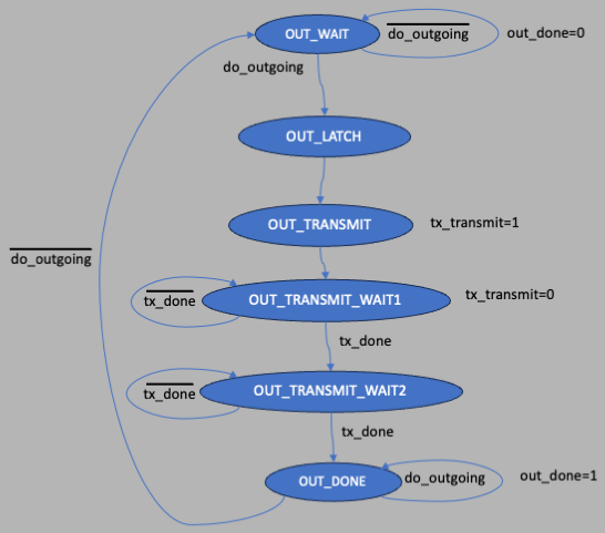
with the following code:
    //
    //  now make the state machine to handle sending 16 bit words to the RPi
    //
    localparam [2:0] OUT_WAIT=0, OUT_LATCH=1, OUT_TRANSMIT=2,
        OUT_TRANSMIT_WAIT1=3, OUT_TRANSMIT_WAIT2=4, OUT_DONE=5;
    reg [2:0] out_state;
    reg [15:0] tx_out;
    reg transmit_out;
    reg out_done;
    reg [2:0] outgoing_what;
    always @ (posedge clock25)
        if (reset) begin
            out_state <= OUT_WAIT;
            transmit_out <= 0;
            out_done <= 0;
            tx_out <= 0;
            outgoing_what <= 0;
        end
        else case (out_state)
            OUT_WAIT: begin
                transmit_out <= 0;
                tx_out <= 0;
                out_done <= 0;
                out_state <= do_outgoing ? OUT_LATCH : OUT_WAIT;
                outgoing_what <= rx_instructions[3:1];    // what is going out (only need 3 bits for now)
            end
            OUT_LATCH: begin
                case (outgoing_what)
                    3'b001: tx_out <= adc_data;
                    3'b010: tx_out <= test;
                    3'b011: tx_out <= version;
                    3'b100: tx_out <= control;
                    3'b101: tx_out <= status;
                    3'b110: tx_out <= blast;
                    3'b111: tx_out <= adc_fifo_data_count;
                    default: tx_out <= 16'hDEAD;    // error!
                endcase
                out_state <= OUT_TRANSMIT;
            end
            OUT_TRANSMIT: begin
                transmit_out <= 1;
                out_state <= OUT_TRANSMIT_WAIT1;
            end
            OUT_TRANSMIT_WAIT1: begin
                transmit_out <= 0;
                out_state <= tx_done ? OUT_TRANSMIT_WAIT2 : OUT_TRANSMIT_WAIT1 ;
            end
            OUT_TRANSMIT_WAIT2: begin
                out_state <= tx_done ? OUT_DONE : OUT_TRANSMIT_WAIT2;
            end
            OUT_DONE: begin
                out_done <= 1;
                out_state <= do_outgoing ? OUT_DONE : OUT_WAIT;
            end
        endcase
        assign outgoing_done = out_done;
And now we have to build the state machine that will take data out of the ADC FIFO and send it 16 bits at a time to the RPi. When triggered, the state machine does a FIFO read by toggling read enable high and then low, then latches the 16 bits of output, then sends it 1 byte at a time. Then it increments a counter and checks to see if the counter is at 65535 indicating all data has been sent. If so, it then asserts blast_done and waits for do_blast to go away (handshakes with the OUT state machine). If there's more data to send, it then goes back to reading the FIFO and so on.
One place we have to be careful here: we are going to be blasting data out as fast as possible, and the uart_tx state machine will be sending 1 byte at a time, and doing it twice per 16-bit FIFO word. The BLAST state machine will be looking at the tx_done signal coming out of the uart_tx state machine. We can maybe assume that since both BLAST and uart_tx state machines run with the same 25ns clock, that the tx_done signal will be 1 clock length, but it is ALWAYS is dangerous to make such assumptions. So to protect ourselves we will have the BLAST state machine to first assert transmit, which tells the TX state machine to send the 2 bytes through the uart_tx state machine, then wait for tx_done to be asserted, signalling that the first byte is sent. But then we will wait for tx_done to go to zero, which is an indication that the uart_tx state machine is ready to send another byte. Once tx_done is deasserted, we then wait for it to be asserted again, indicating the second byte has been sent, and then wait for it to be deasserted to indicate all is done. This is perhaps a little bit of overkill and does cost a few 25MHz clock ticks (40ns), but it is always good practice to use the extra time to make sure all circuit modules are in sync.
The state machine should look like this:
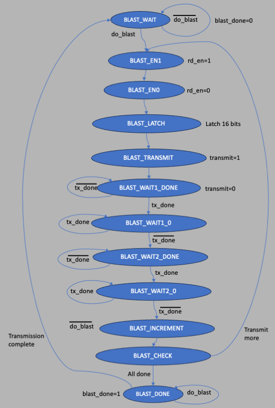
The code will be:
    //
    //  now make the state machine for blasting data back to the RPi.
    //
    //  we will assume that the FIFO is full and just keep emptying it until it's empty
    //
    localparam [3:0] BLAST_WAIT=0, BLAST_EN1=1, BLAST_EN0=2, BLAST_LATCH=3,
        BLAST_TRANSMIT=4, BLAST_WAIT1_DONE=5, BLAST_WAIT1_0=6, BLAST_WAIT2_DONE=7,
        BLAST_WAIT2_0=8, BLAST_INCREMENT=9, BLAST_CHECK=10, BLAST_DONE=11;
    reg [3:0] blast_state;
    reg [15:0] count;
    reg blast_all_done;
    reg [15:0] blast_data;
    reg [15:0] blast_count;
    reg blast_transmit;
    reg data_fifo_wr;
    wire fifo_last = (blast_count == 16'h1);
    wire count_done = count == blast;
    wire all_done = adc_fifo_empty || count_done;
    always @ (posedge clock25)
        if (reset) begin
            count <= 0;
            blast_all_done <= 0;
            blast_transmit <= 0;
            adc_fifo_rd <= 0;
            data_fifo_wr <= 1;
            blast_data <= 0;
            blast_state <= BLAST_WAIT;
        end
        else case (blast_state)
            BLAST_WAIT: begin
                count <= 0;
                blast_all_done <= 0;
                blast_transmit <= 0;
                adc_fifo_rd <= 0;
                data_fifo_wr <= 1;
                blast_data <= 0;
                blast_state <= do_blast ? BLAST_EN1 : BLAST_WAIT;
//                blast_state <= do_blast & adc_fifo_full ? BLAST_EN1 : BLAST_WAIT;
            end
            BLAST_EN1: begin
                //
                //  assert fifo rd enable
                //
                data_fifo_wr <= 0;
                adc_fifo_rd <= 1;
                blast_state <= BLAST_EN0;
            end
            BLAST_EN0: begin
                //
                //  deassert fifo rd enable
                //
                adc_fifo_rd <= 0;
                blast_state <= BLAST_LATCH;
            end
            BLAST_LATCH: begin
                //
                //  data will have upper 12 bits of ADC, then 00, then fifo_empty, then fifo_last
                //
                blast_data <= test_mode ? count :
                    {adc_fifo_data[15:4],2'b00,adc_fifo_empty,fifo_last};
                blast_count <= adc_fifo_data_count;
                blast_state <= BLAST_TRANSMIT;
            end
            BLAST_TRANSMIT: begin
                //
                //  assert the transmit signal, this goes to the TX state machine in TOP
                //  then go to the wait done state and release the blast_transmit so it
                //  doesn't confuse anything.  note that the blast_transmit only happens
                //  once per transmitting 16 bit words so we clear it in the next state
                //
                blast_transmit <= 1;
                blast_state <= BLAST_WAIT1_DONE;
            end
            BLAST_WAIT1_DONE: begin
                //
                //  now wait for tx_done to be asserted, which means the transmission of
                //  the first byte is finished
                //
                blast_transmit <= 0;
                blast_state <= tx_done ? BLAST_WAIT1_0 : BLAST_WAIT1_DONE;
            end
            BLAST_WAIT1_0: begin
                //
                //  wait for the uart_tx state machine to drop tx_done, which tells us that
                //  it's ready to send the next byte
                //
                blast_state <= tx_done ? BLAST_WAIT1_0 : BLAST_WAIT2_DONE;
            end
            BLAST_WAIT2_DONE: begin
                //
                //  2nd byte is being transmitted.  wait for tx_done to signal finished
                //
                blast_state <= tx_done ? BLAST_WAIT2_0 : BLAST_WAIT2_DONE;
            end
            BLAST_WAIT2_0: begin
                //
                //  again wait for tx_done to go away before continuing
                //
                blast_state <= tx_done ? BLAST_WAIT2_0 : BLAST_INCREMENT;
            end
            BLAST_INCREMENT: begin
                //
                //  increment the counter that counts number of 16-bit words sent
                //
                count <= count + 1;
                blast_state <= BLAST_CHECK;
            end
            BLAST_CHECK: begin
                //
                //  check to see we are all done transmitting all FIFO words
                //
                blast_state <= all_done ? BLAST_DONE : BLAST_EN1;
            end
            BLAST_DONE: begin
                //
                //  wait for do_blast to go away before going back to wait state
                //
                blast_all_done <= 1;
                blast_state <= do_blast ? BLAST_DONE : BLAST_WAIT;
            end
        endcase
    assign blast_done = blast_all_done;
    assign adc_fifo_wr = global_start & data_fifo_wr;
    //
    //  now take care of merging OUT_ and BLAST_ uart_tx outputs
    //
    assign tx_transmit = blast_transmit | transmit_out;
    assign tx_transmit_out = do_blast ? blast_data : tx_out;
Note that the state machine waits for do_blast to be asserted, but does
not wait for the ADC FIFO is full. We will therefore require that the software
running in the RPi, control the FIFO using the control register bit 0,
global_start, to control what goes into the FIFO. So the software will
have to first assert global_start to get the FIFO filled up, wait for it
to be filled, then de-assert global_start so that when we drain the FIFO,
we aren't filling it up and that's important because we are filling and reading
the FIFO at different rates! So the transmission of
data back to the RPi stops when all_done is asserted, which happens
when either the ADC FIFO is empty or we've transmitted the amount of data
specified in the blast register.
Also, the line adc_fifo_wr controls whether data can get sent into the ADC FIFO, and is controlled by asserting both global_start (fromt he control register), and the register data_fifo_wr, which is set to 1 when the BLAST state machine is idle and set to zero while it is being drained. The last few lines of the above code are because we will be sending data out from 2 different state machines, so we have to merge the functionality that the TX state machine needs (tx_transmit and the 16 bits of data which go into the output register tx_transmit_out).
The final bit of code in controller is to push a bunch of signals into the debug output of controller.v so that top.v can send them to various outputs for debugging.
    assign debug = {
        //  49      adc_fifo_empty
        //  48      count_done
        //  47:32   tx_transmit_out[15:0]
        //  31      do_outgoing
        //  30      transmit_out
        //  29      blast_transmit
        //  28       blast_done
        //  27       do_blast,
        //  26:23     blast_state[3:0]
        //  22      tx_done
        //  21      tx_transmit
        //  20      out_done
        //  19:17   out_state[2:0]
        //  16      in_done
        //  15      in_read_fifo
        //  14:12   in_state[2:0]
        //  11      do_incoming
        //  10      do_blast
        //  9       incoming
        //  8       rx_instructions[7]
        //  7:5     rx_instructions[3:1]
        //  4:1     rx_state
        //  0       clock25
        adc_fifo_empty,count_done,                                                      //  49,48
        tx_transmit_out[15:0],                                                          //  47:32
        do_outgoing,                                                                    //  31
        transmit_out,blast_transmit,blast_done,do_blast,blast_state[3:0],               //  30:23
        tx_done,tx_transmit,out_done,out_state[2:0],in_done,                            //  22:16
        in_read_fifo,in_state[2:0],do_incoming,do_blast,incoming,rx_instructions[7],    //  15:8
        rx_instructions[3:1],rx_state[3:0],clock25};                                    //  0:7
And the final bit of code to finish top.v is to first instantiate the controller module:
    //
    //  now instantiate the controller
    //
    wire global_state;
    wire [49:0] cdebug;
    controller CONTROL (
        .clock25(clock25),
        .fifo_clock(fifo_clock),
        .reset(reset),
        .global_start(global_start),
        .rx_fifo_empty(rx_empty),
        .rx_fifo_data(rx_dout),
        .rx_fifo_rd_en(rx_rd_en),
        .tx_transmit_out(transmit_word),
        .tx_transmit(begin_transfer),
        .tx_done(tx_done),
        .version(VERSION),
        .test(sw),
        .adc_data(r_adc_data),
        .adc_fifo_empty(fifo_empty),
        .adc_fifo_full(fifo_full),
        .adc_fifo_rd(rd_en),
        .adc_fifo_wr(wr_en),
        .adc_fifo_data_count(fifo_data_count),
        .adc_fifo_data(dout),
        .debug(cdebug)
    );
Next, we assign values to the output led for monitoring:
    assign led[0] = rx_empty;
    assign led[1] = rx_full;
    assign led[2] = fifo_data_count == 12'h1;
    assign led[3] = fifo_empty;
    assign led[4] = fifo_full;
    assign led[5] = global_start;
    assign led[15] = clock_1hz;             // make a heartbeat
and to assign signals to the JA and JB output for debugging:
        //  49      adc_fifo_empty
        //  47:32   tx_transmit_out[15:0]
        //  31      do_outgoing
        //  30       transmit_out
        //  29       blast_transmit
        //  28       blast_done
        //  27       do_blast,
        //  26:23     blast_state[3:0]
        //  22      tx_done
        //  21      tx_transmit
        //  20      out_done
        //  19:17   out_state[2:0]
        //  16      in_done
        //  15      in_read_fifo
        //  14:12   in_state[2:0]
        //  11      do_incoming
        //  10      do_blast
        //  9       incoming
        //  8       rx_instructions[7]
        //  7:5     rx_instructions[3:1]
        //  4:1     rx_state
        //  0       clock25
    always @*
        case (sw[12])
            0: JA = {rx_rd_en,rx_empty,rd_en,tx_done,tx,dv,rx,clock25};
            1: JA = {cdebug[10],rd_en,wr_en,fifo_empty,tx,fifo_full,rx,clock25};
        endcase
    always @*
        case (sw[15:13])
            3'b000: JB = dout[15:8];
            3'b001: JB = dout[7:0];
            3'b010: JB = dout[11:4];
            3'b011: JB = {tx_done,cdebug[28],cdebug[49],cdebug[48],cdebug[26:23]};
            3'b100: JB = cdebug[39:32];
            3'b101: JB = cdebug[47:40];
            3'b110: JB = {cdebug[31],cdebug[19:17],cdebug[35:32]};
            3'b111: JB = cdebug[7:0];
        endcase
The above project archive can be found here.
RPi Python code
The python code we need is very similar to the previous python programs, in that we will be using the tkinter GUI, but since we want to make plots of voltages as a function of time for a large amount of data, we should switch to the matplotlib plotting code, which is much faster. You can find the code here. When you run it, you will see the following:
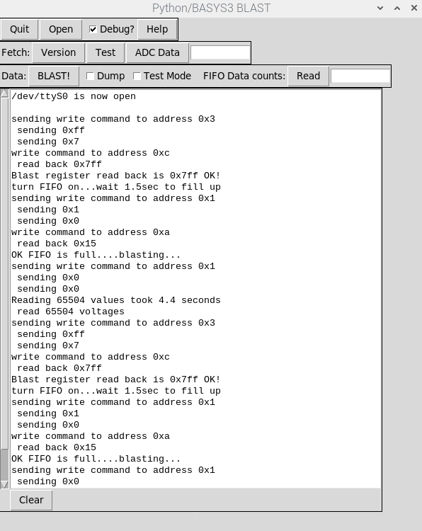
The top row that starts with "Fetch" is for the usual fetching of 16-bit data. The next 2 rows allow you to read the Status Register (it's read only) and the 2 rows after that are for the Control Register followed by the Blast Register (which contains the number of 16-bit words to "blast" to the RPi). Below the Blast Register is a row that allows access to the Data. To keep things working smoothly, the "BLAST!" button does all the work necessary to fill the FIFO with 65535 consecutive data points and read it out and plot it. All you need to do is to run the python script and push the "BLAST!" button. The sequence that happens when you do so is this:
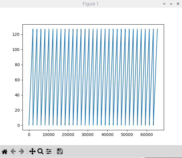
The plot will show all 65535 values, so you should use the zoom feature to see details. In the figure below, you can see the ensuing plot when run in test mode. Here you see each of the 32 counters go from 0 to 128 (remember, each ADC value gets divided by 16, shifting away the bottom 12 bits). The following figure shows the resulting plot.
The whole thing should take around 4-5 seconds for the entire 65535 words.
If you use the SAELE logic analyzer and set the FPGA slide switches so that the upper 5 switches are all down, then the logic analyzer upper 8 bits will show you the transactions as in the following screen shot:
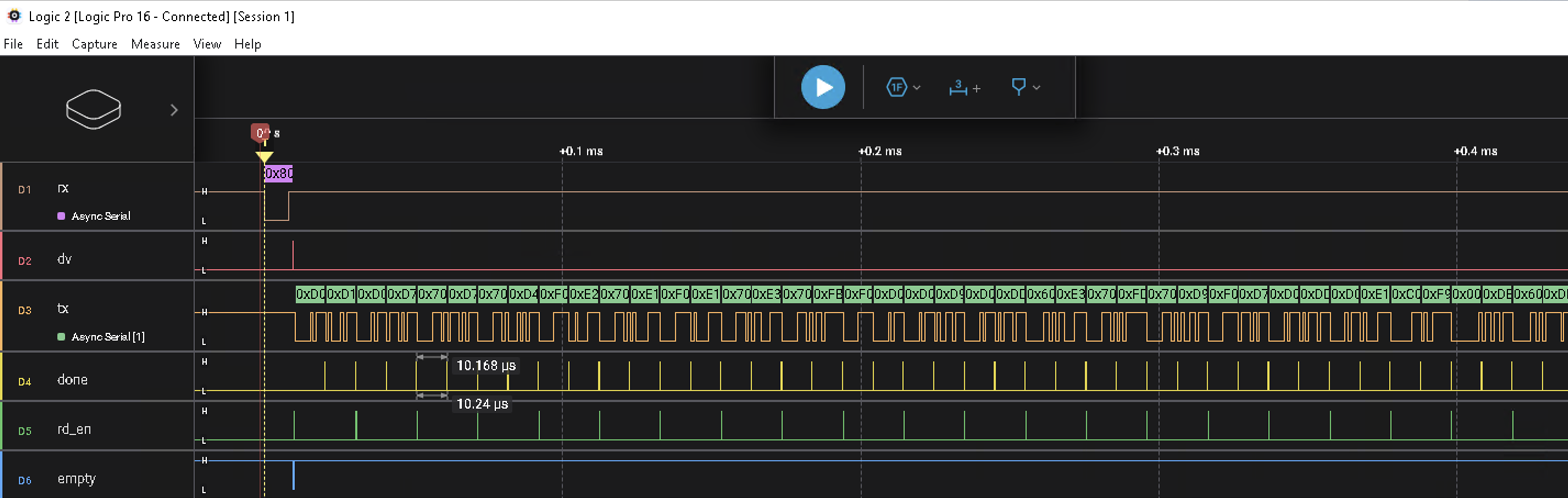
The upper trace labeled "rx" is configured as an "async serial" line, so that the logic analyzer software will decode it, and it shows that the line is sending 0x80 which is the correct code for "blasting". The next line is "dv", or data valid, telling the FPGA state machines that data has arrived and is put into the RX FIFO. The signal labeld "empty" is telling you that that FIFO is no longer empty. This is the signal to the "RX" state machine in the controller.v to do its thing, which is to decode the incoming byte and start blasting data back. The 3rd line labeled "tx" shows the data being sent back 1 byte at a time. The "done" line is the signal from the uart_tx module that it sent a byte, so we should have 2 of those asserted for every 16 bit words. Notice that the signal "rd_en" is the read enable into the DATA FIFO, and that signal is asserted once per two "done" assertions, which is what we want. And you can see that the data is being sent as fast as possible, and here it only takes around 1. seconds (65535×2×10μs) to read out everything, quite a speedup from the previous project where at 450μs per transfer it would have taken 45 times longer!