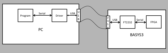
Having an FPGA in a development kit like the BASYS3 can be very useful if you are planning to use it for data acquisition. And to do that, we need some kind of communication path between the FPGA and a computer. The BASYS3 does have 2 USB connectors: a micro-USB on J4 and a macro-USB (standard USB connector) on J2. The latter is not really useful for I/O, it's more intended to be used for connecting a mouse or keyboard (see page 7 of basys3_rm.pdf for more).
The micro-USB connector (J4) is the one we will focus on. The board side of this connector has a chip that bridges USB to a serial port, the chip is from a company called FTDI ( Future Techynology Devices International Ltd), which specializes in gadgets that allow you to use USB connections for various products. The chip on board is the FT2232HQ USB-UART bridge, and the data sheet can be found here. Basically, what it does is to allow you to connect using USB, and "tunnel" serial port data through to the FPGA. So the communication path between the PC and the BASYS3 board is via a serial connection, tunneled inside USB.
The communication path is as in the next figure:
One of the easiest ways to communicate with hardware (like FPGAs) is via
serial communication links. This is quite common for computers, with many
protocols to choose from, all more or less the same. The one we will use is
called UART, which traces its orgin back to the 1960s.
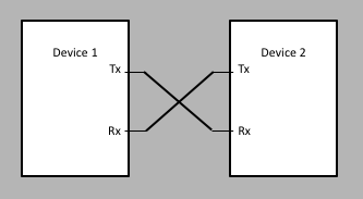
Serial links such as UART (universal asynchronous receiver-transmitter)
are very simple, and allows 2 circuits to communicate. Each circuit has a
receive line and a separate transmit line. The transmit line of one circuit is
connected to the receive of the other, and vice versa.
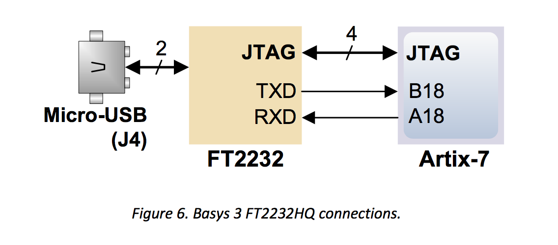
There are 2 ways we can get a computer to communicate with the BASYS3 board using
a UART serial connection: 1) connect the computer to the BASYS3 via a USB cable,
and have the UART communication "piggy back" through USB; 2) have rx and
tx lines. This is described
on page 7 of the BASYS3 manual in figure 6:
This figure shows the 2 lines serial lines that are connected to the FPGA on
pins B18 (receive) and A18 (transmit).
All you have to do is route these into the FPGA by adding to the .xdc file
(see below).
The second way is described in the next figure, where you make a direct connection
of the transmitting signal from one device to the receiving port on the other, and
vice versa:
In this tutorial we will use the first way, but the FPGA will still be driving
tx and looking at rx for both methods. So in our project, we will
have 1 input to the top level module called rx and one output called
tx, and we will use the B18 and A18 pins for these which means the FPGA will
be talking to the FT2232 chip. In this case, the Artix-7 FPGA is transmitting,
but the FT2232 is
receiving, hence tx from the FPGA is connected to RXD on the FT2232.
Decoding and encoding UART is simple once you understand the time structure.
Let's consider the tx line first. This line is the transmitter, from the point of
view of the FPGA.
In all serial links, the information is sent one bit at a time. From the point
of view of the receiver, there is a single line where the data is flowing in,
and on this line it needs to know when data is coming, what the time period is for each bit,
and what protocol it has to use to decode the data.
The transmitting and receiving devices have to both agree in advance somehow what the
parameters are.
For the UART, we have the following rules:
This kind of error detection is only useful if there is a
single bit flip - 2 bits flipped will not change the parity! And the error detection will
only tell you that an error was present, it will not allow you to know which of the
sent bits is wrong. To perform error detection and correction, you have to use
a higher order technique, and usually this means adding another byte (or more) to
the transmission stream that will be be used for redundancy checking and correction.
This is not covered in this tutorial.
For this project, we will use a serial receiver and transmitter that will use 1
start bit, 1 stop bit, and no parity, and the transmitter
will send 1 byte at a time with no apparent limit on the number of bytes
the receiver can take. You can write
your own verilog to implement this, but if you want to use one that has been
debugged, you can find them below with explanations of how to use them.
Your top level module (call this top.v) will have the following ports:
Talking to FPGAs over Serial Ports
So we have to have agreement on both sides on
The timing diagram is shown below. Note that parity bits are optional, and the stop
bit can be 1, 1.5, or 2 bits wide. It's all up to the programmer, but of course the
transmitter and receiver have to agree.
module top (
    input clock,
    input reset,
    input transmit,
    input [7:0] sw,
    input rx,
    output tx,
    output reg [7:0] led
);
The transmit and reset are push buttons on the BASYS3 board. Let's use
BTNL for the transmit and BTNR for reset, which means that you can look on
page 16 of the BASYS3 manual and see that
BTNL is pin W19 and BTNR is T17. Note that the clock is pin W5, so in the constraints you put
the following:
## clock
set_property PACKAGE_PIN W5 [get_ports clock]
set_property IOSTANDARD LVCMOS33 [get_ports clock]
##
## reset
set_property PACKAGE_PIN T17 [get_ports reset]
set_property IOSTANDARD LVCMOS33 [get_ports reset]
##
## transmit
set_property PACKAGE_PIN W19 [get_ports transmit]
set_property IOSTANDARD LVCMOS33 [get_ports transmit]
Next, we will need to debounce the transmit signal, so that if you drink too much coffee you won't end up sending too many bytes! We can use the same debouncer.v circuit from the previous project and instantiate it like this:
    //
    //  debounce the transmit push button
    //
    wire transmit_level, transmit_pulse;
    debouncer DEBOUNCE (
        .clock(clock),
        .button(transmit),
        .level(transmit_level),
        .pulse(transmit_pulse)
        );
We will be using transmit_pulse to trigger sending a byte from the FPGA to the RPi.
Serial Transmission
The verilog code for the UART serial transmitter can be found
here.
Usage is relatively simple. For the transmitter, you have the following ports:
   input        i_Clock,
   input [15:0] i_Clocks_per_Bit,
   input        i_Reset,
   input        i_Tx_DV,
   input [7:0]  i_Tx_Byte,
   output       o_Tx_Active,
   output reg   o_Tx_Serial,
   output       o_Tx_Done,
   output [7:0] o_debug
Inputs are:
Outputs are:
We won't be using the o_debug output so we can leave it out and the synthesizer won't bring those signals out.
The instantiation inside your top level module will look something like this:
    //
    //  instantiate uart_tx
    //
    wire active, done;
    uart_tx TX (
        .i_Clock(clock),
        .i_Clocks_per_Bit('d100),
        .i_Tx_DV(transmit_pulse),
        .i_Reset(reset),
        .i_Tx_Byte(sw),
        .o_Tx_Serial(tx),
        .o_Tx_Active(active),
        .o_Tx_Done(done)
    );
The way the uart_tx module works is that the line i_Tx_Serial is active low, so it starts out high. The state machine will wake up when i_Tx_DV is asserted, and drive o_Tx_Active high. It then sends the start bit by driving i_Tx_Serial low for some number of clock cycles determined by the input i_Clocks_per_Bit, then will send each of the 8 bits by asserting i_Tx_Serial as appropriate for i_Clocks_per_Bit clock cycles each. After that it will drive i_Tx_Serial high for i_Clocks_per_Bit clock cycles, which would be interpreted as the stop bit, and finish by asserting o_Tx_Done for 1 clock cycle (10ns), and drive o_Tx_Active low. The transmission is finished.
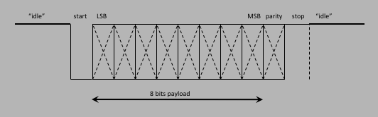
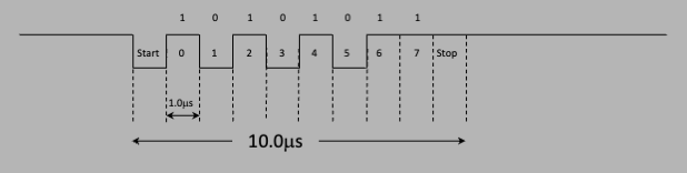
As an example, say you want to send the bit pattern 'b11010101 (0xD5) with a baud rate of 1000000 (106bps, what we will be using here). The whole transaction should look like the following figure, which each bit being 1.0μs long:
   input        i_Clock,
   input [15:0] i_Clocks_per_Bit,
   input        i_Reset,
   input        i_Rx_Serial,
   output       o_Rx_DV,
   output [7:0] o_Rx_Byte,
   output [7:0] o_debug
Inputs are:
Instantiation would look like this:
    //
    //  instantiate uart_rx
    //
    wire dv;
    wire [7:0] rx_data;
    uart_rx RX (
        .i_Clock(clock),
        .i_Clocks_per_Bit('d100),
        .i_Reset(reset),
        .i_Rx_Serial(rx),
        .o_Rx_DV(dv),
        .o_Rx_Byte(rx_data)
        );
    always @ (posedge dv) led <= rx_data;
For the uart_tx module, the i_Tx_DV line initiates the transfer.
Both of these verilog modules were from opencores, but needed a few changes in order to work in this tutorial. The code above have been tested and verified inside the BASYS3 board.
For the constraints file, the pin for rx and tx will be:
##USB-UART Interface
set_property PACKAGE_PIN A18 [get_ports tx]
set_property IOSTANDARD LVCMOS33 [get_ports tx]
set_property PACKAGE_PIN B18 [get_ports rx]
set_property IOSTANDARD LVCMOS33 [get_ports rx]
One last thing: let's setup a "heartbeat", a signal that tells us that the firmware is working. The easiest thing to do is to make an LED blink at around 1Hz. Our clock is 10ns, and if we want a 1s heartbeat, we would need a counter that can count up to 108 counts. So we would need to solve the equation 2N=108, and the solution is N=8/log(2)=26.6. So if we have a 27 bit counter, and use the MSB for the heartbeat and send it to one of the LEDs, that should do it.
Let's add
output heartbeat
to the top.v module input/outputs, and the counter and heartbeat code like this:
    reg [27:0] counter;
    always @ (posedge clock) counter <= counter + 1;
    assign heartbeat = counter[27];
And, to the tdc constraints file, we would add the following to tie the heartbeat
to the top LED, which is at pin L1:
##
## heartbeat
set_property PACKAGE_PIN L1 [get_ports heartbeat]
set_property IOSTANDARD LVCMOS33 [get_ports heartbeat]
The full top.v module should look like this:
`timescale 1ns/1ps

module top (
    input clock,
    input reset,
    input transmit,
    input [7:0] sw,
    input rx,
    output tx,
    output reg [7:0] led,
    output heartbeat
);
    reg [27:0] counter;
    always @ (posedge clock) counter <= counter + 1;
    assign heartbeat = counter[27];
    //
    //  debounce the transmit push button
    //
    wire transmit_level, transmit_pulse;
    debouncer DEBOUNCE (
        .clock(clock),
        .button(transmit),
        .level(transmit_level),
        .pulse(transmit_pulse)
        );

    //
    //  instantiate uart_tx
    //
    wire active, done;
    uart_tx TX (
        .i_Clock(clock),
        .i_Clocks_per_Bit('d100),
        .i_Tx_DV(transmit_pulse),
        .i_Reset(reset),
        .i_Tx_Byte(sw),
        .o_Tx_Serial(tx),
        .o_Tx_Active(active),
        .o_Tx_Done(done)
    );
    //
    //  instantiate uart_rx
    //
    wire dv;
    wire [7:0] rx_data;
    uart_rx RX (
        .i_Clock(clock),
        .i_Clocks_per_Bit('d100),
        .i_Reset(reset),
        .i_Rx_Serial(rx),
        .o_Rx_DV(dv),
        .o_Rx_Byte(rx_data)
        );
    always @ (posedge dv) led <= rx_data;

endmodule
The full top.xdc pin file will have the above clock, reset,
transmit, rx, and tx pins, plus the 8 pins for the leds
and the 8 slide switches:
## clock
set_property PACKAGE_PIN W5 [get_ports clock]
set_property IOSTANDARD LVCMOS33 [get_ports clock]
##
## reset
set_property PACKAGE_PIN T17 [get_ports reset]
set_property IOSTANDARD LVCMOS33 [get_ports reset]
##
## transmit
set_property PACKAGE_PIN W19 [get_ports transmit]
set_property IOSTANDARD LVCMOS33 [get_ports transmit]
##
## heartbeat
set_property PACKAGE_PIN L1 [get_ports heartbeat]
set_property IOSTANDARD LVCMOS33 [get_ports heartbeat]
##
##USB-UART Interface
set_property PACKAGE_PIN A18 [get_ports tx]
set_property IOSTANDARD LVCMOS33 [get_ports tx]
set_property PACKAGE_PIN B18 [get_ports rx]
set_property IOSTANDARD LVCMOS33 [get_ports rx]
##
## Switches
set_property PACKAGE_PIN V17 [get_ports {sw[0]}]
set_property IOSTANDARD LVCMOS33 [get_ports {sw[0]}]
set_property PACKAGE_PIN V16 [get_ports {sw[1]}]
set_property IOSTANDARD LVCMOS33 [get_ports {sw[1]}]
set_property PACKAGE_PIN W16 [get_ports {sw[2]}]
set_property IOSTANDARD LVCMOS33 [get_ports {sw[2]}]
set_property PACKAGE_PIN W17 [get_ports {sw[3]}]
set_property IOSTANDARD LVCMOS33 [get_ports {sw[3]}]
set_property PACKAGE_PIN W15 [get_ports {sw[4]}]
set_property IOSTANDARD LVCMOS33 [get_ports {sw[4]}]
set_property PACKAGE_PIN V15 [get_ports {sw[5]}]
set_property IOSTANDARD LVCMOS33 [get_ports {sw[5]}]
set_property PACKAGE_PIN W14 [get_ports {sw[6]}]
set_property IOSTANDARD LVCMOS33 [get_ports {sw[6]}]
set_property PACKAGE_PIN W13 [get_ports {sw[7]}]
set_property IOSTANDARD LVCMOS33 [get_ports {sw[7]}]
##
## LEDs
set_property PACKAGE_PIN U16 [get_ports {led[0]}]
set_property IOSTANDARD LVCMOS33 [get_ports {led[0]}]
set_property PACKAGE_PIN E19 [get_ports {led[1]}]
set_property IOSTANDARD LVCMOS33 [get_ports {led[1]}]
set_property PACKAGE_PIN U19 [get_ports {led[2]}]
set_property IOSTANDARD LVCMOS33 [get_ports {led[2]}]
set_property PACKAGE_PIN V19 [get_ports {led[3]}]
set_property IOSTANDARD LVCMOS33 [get_ports {led[3]}]
set_property PACKAGE_PIN W18 [get_ports {led[4]}]
set_property IOSTANDARD LVCMOS33 [get_ports {led[4]}]
set_property PACKAGE_PIN U15 [get_ports {led[5]}]
set_property IOSTANDARD LVCMOS33 [get_ports {led[5]}]
set_property PACKAGE_PIN U14 [get_ports {led[6]}]
set_property IOSTANDARD LVCMOS33 [get_ports {led[6]}]
set_property PACKAGE_PIN V14 [get_ports {led[7]}]
set_property IOSTANDARD LVCMOS33 [get_ports {led[7]}]
Putty is the name of an all purpose serial port terminal program that
has mostly outlasted its usefulness since the early 2000s. But for us,
it can work to make sure that we have a good communication path to the
BASYS3 board, for both transmitting and receiving. You should be able
to download putty onto your PC (running Windows of course).
To use it, first make sure that the FPGA on the BASYS3 is programmed
correctly. Then you can run putty.
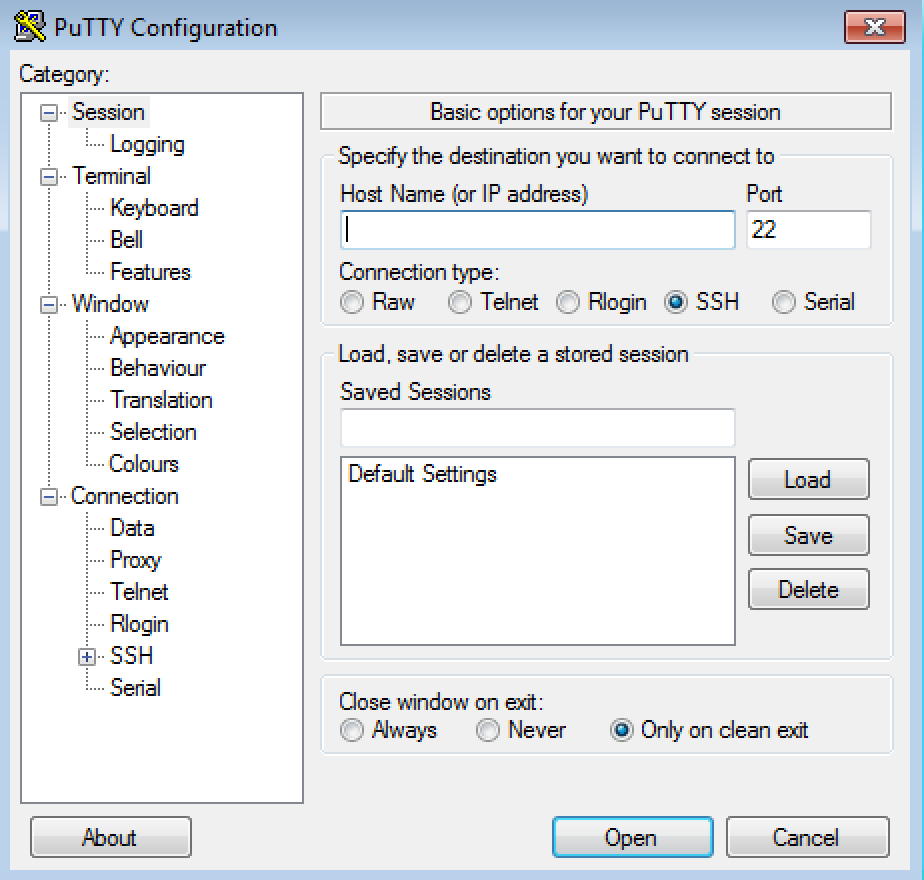
You should see the following window appear:
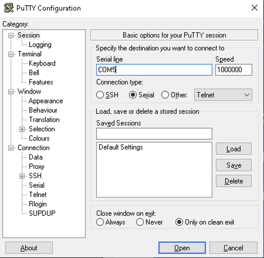
If you don't see that window, you should see the "Category" panel on
the left, click on "Session". Then in the panel on the right side,
click on "Serial", it should look like this:
You should set the "Speed" to 1000000 (the default
baud rate in the FPGA code, or whatever you might have changed it to),
and the "Serial line" to something that depends on your computer.
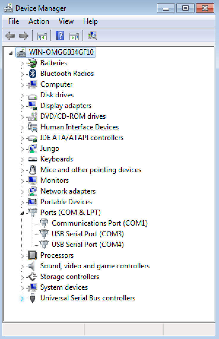
This is where putty can be a pain - it does not necessarily know which
COM port the device manager has mapped the USB connection to. You can
look in the device manager to find out however by right clicking on the
"Computer" desktop icon, and clicking on "Device Manager" for Windows 7.
Then open up the "Ports (COM & LPT)" to see what's there. You should
see something like this:
I don't know why there are 2 USB Serial ports open, but one of them
will work and the other won't (in this example, COM4 works but COM3
does not).
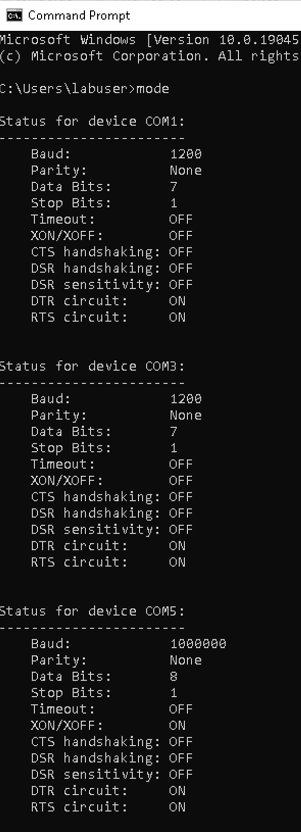
Another possibility is to run the "cmd" Windows command (or
Powershell) and type "mode" at the prompt. You should see
something like this:
So you would try COM1, COM3, or COM5 in the putty serial port
window under "Serial line" and
hit "OK", and you should see a blank terminal window pop
up, like this:
Connecting to a PC
![]()