Here we will make 2 projects: one to blink the LEDs and 1 to show how to use the 4-digit LED display (here). A special tutorial on how to program the flash ram is found here.
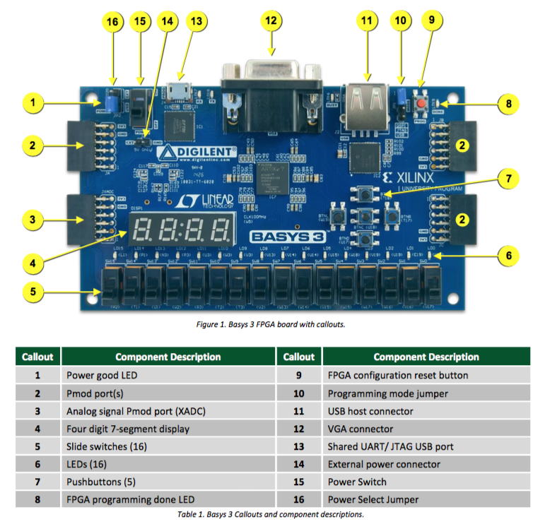
It's a good idea to have the BASYS3 board reference manual around, which you can find here, or just grab it directly from here. In the reference manual you will find all sorts of useful information on how to connect BASYS3 things like switches, LEDs, etc to the FPGA. For these two projects, it's a good idea to familiarize yourself with the board, shown here:
The first thing we will do is to build a project that sets up a clock and counters to blink some of the LEDs. Runing Vivado 2017.2, you should see the same picture as described above. Click on "Create Project", and go through the "New Project" wizard, and specify a new project which you can call "blinking". This will be a "RTL Project", check "do not specify sources at this time", and that will get you to the "Default Part" menu. Now we have to specify the exact FPGA part we are using. You can find this in the "basys3_rm.pdf" file on the first page: XC7A35T-1CPG236C: "XC7A" means Artix-7 model, 35T is the specific part (the Artix-7 comes in many sizes), the "-1" is a mistake (it should be at the end of the model, it's the speed designation) and CPG236 is the "form factor" (this determines how it's attached to the board). So you should choose "xc7a35tcpg236-1" in the "Default Part" window and hit "next", and then hit finish. You will get a fresh window with nothing in it, like what is shown below:
Click on the "+" in the "Sources" panel, "Add or create design sources", "Create File", call it "TOP" (or whatever you wish), hit "OK", and then "Finish". It will next ask you to specify IO Ports, just hit OK there and answer "Yes" to the next question. It will then show you the file "TOP.v" under the "Design Sources(1)" item in the "Sources" panel.
Double click on "TOP (TOP.v)" and edit the source file. It will empty except for the `timescale 1ns/1ps directive at the top, some comments that you can erase or leave, and the module declaration:
    module TOP(

        );
    endmodule
Let's specify the IO ports next. We want to blink all of the LEDs at
different rates, so we will need 1 clock, and 16 LEDs. The specifications
could look like this:
    module TOP(
        input clock,
        output [15:0] LED
        );
    endmodule
The BASYS3 board has an onboard 100MHz crystal oscillator that we can use,
it's wired up to the FPGA already. More on that later, it's described
in the basys3_rm.pdf file on page 6. The LEDs are described on page 15,
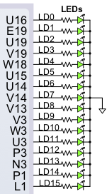
the relevant part of the diagram is shown here:
We want to blink the LEDs so we can see them. We will do this by defining a counter, and tieing each LED to one of the counter bits. Let's say that the slowest LED will blink at around once every 5 seconds, or 0.2Hz. Each subsequent LED will blink x2 faster, which gives 0.4Hz, 0.8Hz, 1.6Hz, etc. 16 bits is quite a large dynamic range, so some of the faster LEDs probably won't be seen as blinking, but that's ok for a first project. For a 100MHz clock, each "tick" is 10ns, so we will need 108 ticks to get something that ticks every 1 second. If we want a tick every 5 seconds, we want something like 4×10⁸ ticks, so we want to solve the equation 2N=4×10⁸, which comes out to N=28.6. This says we need a 29-bit counter. So the code will look like this:
    module TOP(
        input clock,
        input reset,
        output [15:0] LED
        );

    //
    //  make a 29 bit register so we can count to a few seconds
    //  using the 10ns system clock
    //
    reg [28:0] counter;
    always @ (posedge clock)
        if (reset) counter <= 0;
        else counter <= counter + 1;
    assign LED = counter[28:13];
    endmodule
To blink the LEDs, we use the "assign" statement, and tie the
LED lines to the upper 16 bits of the counter. The statement
assign LED = counter[28:13];
means that the synthesizer will take all 16 bits of the LED and assign them
1x1 to each successive bit of counter. So LED[0] is driven
by coutner[13] and so on. You could also have specified this more
clearly by:
assign LED[15:0] = counter[28:13];
but the Vivado synthesizer figures it out if you leave off the [15:0] part.
We've added a "reset" line, and we can deside later how to assign this to something on the board, like one of the push buttons (having a reset line makes simulation easier). The counter is defined using the "reg" type, the reset is synchronous with the clock, and the counter counts up. When it gets to all 1's, it will turn over, which is perfectly fine for these purposes.
Now you are ready to check if the syntax is correct. If you click on "Run Synthesis" in the left most "Flow Navigator" panel, it will run the actual synthesis and report any errors. It will first ask you which "run" you want to launch, just hit "OK" at that first question. You should see "Running synth_design" with a circling progress indicator in the upper right hand corner of the window. If everything worked ok, it should say "Synthesis Complete" with a green check mark, and come up with a "Synthesis Completed" pop-up window asking you want you want to do next. Just hit "Cancel" there.
Next we want to specify the IO pins that the code will use for the inputs and outputs. To do this you first have to find out what pins on the FPGA they are connected to. For the clock, section 4 of basys3_rm.pdf (page 6) tells you it is pin "W5". For the reset, let's use one of the push buttons, which are specified in section 8 ("Basic I/O"), at the top of page 15. If you look closely at the board, you will see each of the buttons has a label. Of the 5 buttons, there are "BTNL", "BTNU", "BTNR", "BTND", and "BTNC" for left, up, right, down, and center. Let's use the upper one, "BTNU", which on page 15 is at pin T18. Also on page 15 it shows the 16 LED pins (from MSB to LSB) as L1, P1, N3, P3, U3, W3, V3, V13, V14, U14, U15, V18, V19, U19, E19, U16. Notice also that the circle shows each LED connected to the FPGA through a resistor on one side, and ground on the other. This means that when the FPGA signal is 1, the LED will turn on.
Now we have to set up the source file that specifies the IO pins. This file is special, and plays a key role in the project. To make it, go back to the "Sources" panel and click the "+" sign again. In the "Add Sources" window, change the radio button to "Add or create constraints" and hit "Next", then click "Create File", give it a name (might as well use the same name, "TOP"), and click "Finish". Now you have to edit it. In the "Sources" panel, you should see "> Constraints (1)", click on the ">" and it should expand and you should see "TOP.xdc". That's the file you want to edit. Double click, taking you into an empty file.
The syntax is a bit obscure, but the good thing is that once you get it correct once, you never have to change it! The thing to understand is that you have to match the pin (e.g. "W5" for the clock) to the IO name in your source (here it's "clock"). So to do this, type the following:
    set_property PACKAGE_PIN W5 [get_ports clock]
    set_property IOSTANDARD LVCMOS33 [get_ports clock]
The first line ties pin "W5" to the port "clock", and the 2nd line sets the
IO "standard" to LVCMOS33, which means low voltage CMOS at 3.3 volts. That
means that the clock signal will toggle below 3.3V and above 3.3V to
differentiate 0 from 1. This is the usual standard for this chip (there
are others, more on that some other time).
Next do the same thing for the reset line, and the 16 LEDs. It should look like this:
## clock
set_property PACKAGE_PIN W5 [get_ports clock]
set_property IOSTANDARD LVCMOS33 [get_ports clock]
##
## reset
set_property PACKAGE_PIN T18 [get_ports reset]
set_property IOSTANDARD LVCMOS33 [get_ports reset]
##
## 16 LEDs
set_property PACKAGE_PIN L1 [get_ports {LED[15]}]
set_property IOSTANDARD LVCMOS33 [get_ports {LED[15]}]
set_property PACKAGE_PIN P1 [get_ports {LED[14]}]
set_property IOSTANDARD LVCMOS33 [get_ports {LED[14]}]
set_property PACKAGE_PIN N3 [get_ports {LED[13]}]
set_property IOSTANDARD LVCMOS33 [get_ports {LED[13]}]
set_property PACKAGE_PIN P3 [get_ports {LED[12]}]
set_property IOSTANDARD LVCMOS33 [get_ports {LED[12]}]
set_property PACKAGE_PIN U3 [get_ports {LED[11]}]
set_property IOSTANDARD LVCMOS33 [get_ports {LED[11]}]
set_property PACKAGE_PIN W3 [get_ports {LED[10]}]
set_property IOSTANDARD LVCMOS33 [get_ports {LED[10]}]
set_property PACKAGE_PIN V3 [get_ports {LED[9]}]
set_property IOSTANDARD LVCMOS33 [get_ports {LED[9]}]
set_property PACKAGE_PIN V13 [get_ports {LED[8]}]
set_property IOSTANDARD LVCMOS33 [get_ports {LED[8]}]
set_property PACKAGE_PIN V14 [get_ports {LED[7]}]
set_property IOSTANDARD LVCMOS33 [get_ports {LED[7]}]
set_property PACKAGE_PIN U14 [get_ports {LED[6]}]
set_property IOSTANDARD LVCMOS33 [get_ports {LED[6]}]
set_property PACKAGE_PIN U15 [get_ports {LED[5]}]
set_property IOSTANDARD LVCMOS33 [get_ports {LED[5]}]
set_property PACKAGE_PIN W18 [get_ports {LED[4]}]
set_property IOSTANDARD LVCMOS33 [get_ports {LED[4]}]
set_property PACKAGE_PIN V19 [get_ports {LED[3]}]
set_property IOSTANDARD LVCMOS33 [get_ports {LED[3]}]
set_property PACKAGE_PIN U19 [get_ports {LED[2]}]
set_property IOSTANDARD LVCMOS33 [get_ports {LED[2]}]
set_property PACKAGE_PIN E19 [get_ports {LED[1]}]
set_property IOSTANDARD LVCMOS33 [get_ports {LED[1]}]
set_property PACKAGE_PIN U16 [get_ports {LED[0]}]
set_property IOSTANDARD LVCMOS33 [get_ports {LED[0]}]
Save these changes. The program should look something like this:
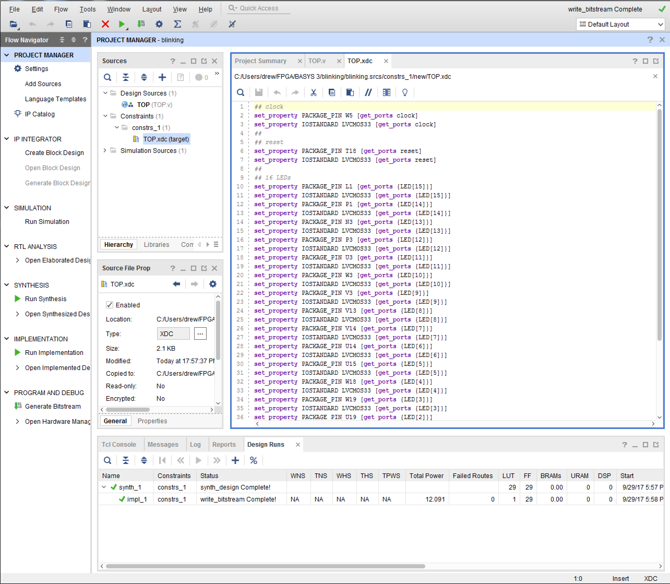
Now you are ready to build it. On the left, in the "Project Manager" panel, you will see "IP INTEGRATOR", "SIMULATION", "SYNTHESIS", "IMPLEMENTATION", and "PROGRAM AND DEBUG". Under them are the operations you can click on. If you click on "Generate Bitstream" under "PROGRAM AND DEBUG", it will realize that you've not run the synthesis or implementation stage, and will ask you if you want to do that by putting up a pop-up window that will say something about how the "Synthesis if out-of-date" and ask if you want to run both synthesis and implementation. Say "Yes", and it will probably put up another window called "Launch Runs". Say "OK" to that one as well. It will then run the synthesizer, followed by the place-and-route, if there are no errors, and then it will make the "bit file". This is a file that can be downloaded to the FPGA over USB.
Now go back to the documentation basys3_rm.pdf, and look in section 2 "FPGA Configuration". It details 3 ways to program the board: using a serial protocol called "JTAG", storing a file in the SPI flash chip, or transferring from a USB memory stick. We want to connect our FPGA to our computer using the USB connection, and program using JTAG. To do this, look for the 4-pin jumper to the right of the USB connector (upper right when holding the board so that the VGA connector is on the upper side) called JP1. It will have 4 pins and a blue jumper. You want to make sure the blue jumper is connecting the middle 2 pins together.
Next, to make sure that the USB will work, you have to look for the 3-pin jumper JP2 and set it to "USB". This will tell the board to draw its power from the USB connection, and you have to make sure that you are using the microUSB connector right next to the on/off switch. Now you are ready to connect the board to your computer via USB.
Back to Vivado, if all is well you should see a popup window called "Bitstream Generation Completed". It wants to know what you want to do next. Check "Open Hardware Manager" and hit OK. That will open up the "Open Hardware Manager" tab on the left panel, and under it you should see "Open Target". Click on that and click on "Auto Connect" when you see that option. If all goes well, the "Program Device" option should now be clickable. When you click on that, it will tell you the devices you can program, which should be your xc7a35t chip. Click on that. It will bring up a window with the name of the bitstream file you made. Click on "Program", and if all goes well you should see a window with a green progress bar. After that, the FPGA will be programmed and you should see the LEDs flashing. Congratulations!
Note that the LEDs to the left are blinking slowly, and the LEDs to the right are not blinking at all. In fact, they are, but they are blinking so fast that you can't see them turn off, so they look like they are all on all the time. If one of the LEDs is off all the time, then either you have a mistake in the xdc file for that LED signal, or the LED is probably just busted. The former is much more likely! Don't forget to try pushing the reset button to make sure that is working properly as well.
In future projects, you might want to set up a "heartbeat" signal. That is, a signal that tells you that the firmware is indeed running. You can now pick the signal heartbeat that you like from the blinking LEDs you see here.
Now you have to build the code and download into the FPGA. The first step is to run the synthesis tool. What synthesis does is to look at the code, decode it into logic and flip-flops, and set up a list (called a "netlist") of what is connected to what logically. In the "PROJECT MANAGER" window to the left, which should look like this:
click on "Run Synthesis", under the "SYNTHESIS" tab. It might ask some questions, just say yes and go on. You should see "Running synth_design" in the upper right hand corner, plus a circular progress widget spinning.
If there are no code errors, the synthesis will pass, and you will get a window asking you what to do next. It will look something like this:
When implementation is finished, you should see another window pup up. Click on "Generate Bitstream" and hit OK. This will make the file of bits that will actually get downloaded into the FPGA. You will see "Running write_bitstream" in the upper right corner of the Vivado window.
Once that is finished, you will see yet another window. Click on "Open Hardware Manager" and hit OK.
Now you have to connect to the basys3 board over USB with the micro-usb cable plugged into the port near the power switch. You should see the LED above the word "POWER" light up. Vivado has to now connect to it, and you do this by clicking on "Open Target". If this is the first time you are connecting after a powerup, clicking on "Open Target" will show you a popup window. Click on "Auto Connect" as shown below.
You should see a brief flash from a progress bar, and then the following in the "HARDWARE MANAGER" panel (top, next to "PROJECT MANAGER"). It should show that the localhost is connected. Then click on "Program Device". It will open up a little window with "xc7a35t_0" as the only option, which is the basys3 board. Click on that. Now you have to specify the file you want to download. You should see a "Program Device" window pop up, like this:
Make sure that "Bitstream file:" is set correctly, it should point to a subdirectory in the directory you are working. If it's not correct, navigate there. The .bit file is in "../counting.runs/impl_1" where "counting" is the name of the main subdirectory I'm working. Find the file, hit "Program", and it will send the program to the FPGA and run it. If the JP1 jumper is set to "JTAG", you should see 0000 on the display. Hitting the bottom push button of the 5 (in a cross pattern) should increment it.
The above project archive can be found here.
The next project consists of code that will count the number of
times some input was present (like a button pushed),
put the count as a 16-bit binary number into the LEDs,
and display the number of counts as a hex number in the
4-digit LED display. Since we have 16 LEDs and 4 LED segment displays,
we can use a 16 bit counter for our counting.
The 4 7-segment LED displays will be driven from the top level module
and will need 3 outputs: segment[6:0], digit[3:0], and dp. These are
explained below, but for now we just add them.
So your verilog TOP module will need to have the
inputs clk, reset, btnCnt, and the outputs
digit[3:0], segment[6:0], dp, and LED[15:0], so the module
declaration should look like this:
For the input, we use the top push button (BTNU) for counting, and leave
the bottom (BTND) for the reset. The constraints file should then have the
following assignments for the clock and the 2 buttons:
The signal btnCnt will cause a counter to be incremented,
and the value of that counter will be displayed on the LEDs and on
the 4 7-segment LED displays (item 4 in the BASYS3 figure at the top
of this tutorial).
Pushing buttons is notoriously dangerous because of "bouncing",
and in our case, a bounce could be (probably will be) recorded
as a count, which is not what we want.
The basys3 board contains some RC components on the push buttons
that will filter out the high frequency bouncing, but if your finger
bounces (too much coffee?) then it won't filter that out.
If you simply register an input (e.g. the push button
input) with the 100MHz system clock, you might count the bounces when
all you wanted to count was the single push. So we need a circuit
module that will "debouce" the btnCnt button. (We don't
really need one for the reset as a bounced reset won't hurt anything.)
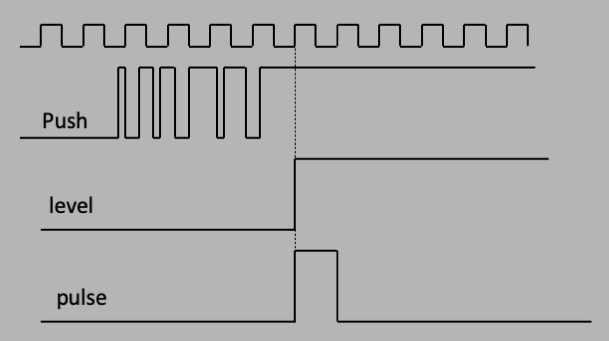
What we want a debouncer circuit to do is to start counting on the
first positive edge of the button pushed, and after a large amount
of time (say 1ms), check if the button is still pushed. If it's
still pushed, then it figures that you meant it to be pushed, and
the circuit outputs a "debounced" signal.
There will be 2 output signals in the code we will write below:
level, the debounced
signal that is asserted as long as the button is pushed; and pulse,
a 1-shot (this is a signal that triggers off of level but is
only up for 1 clock cycle). We will use the system clock
(100MHz) to drive this circuit, so that the pulse signal
generated will be asserted for only 1 clock cycle.
In the figure below, you can see a bouncing signal and what you want
the debouncer to accomplish:
The code for the module is here. Note that the module assumes the clock
is running at 100MHz, so that it can count up to 1ms ('d100000).
The first thing the module does is to register the input with the system
clock, producing ff2. Below that, you can see that if ff2
is high, the counter starts counting but only if the condition
~&count is satisfied. This is a bit of verilog obscurity:
when you have a bus like count[16:0], then if you want to see
if the count is at the maximum, which is when all bits are 1, you
could do the test:
So the code inside the always block is incrementing a counter if the button
has been pushed, and counting up the maximum. If the button has not been
pushed, it decrements the counter down to its minimum value, denoted by
the statement
You can instantiate the debouncer to debounce the btnCnt push
button (the reset is not so important since a bouncing reset will just
reset a lot of times, which doesn't hurt anything).
Next we need some code to count btnCnt presses. We will use the
pulse output fromt he debouncer, btnCnt_1s. Here is where
we instantiate the 16 bit counter, called the_count, and send
the counter value to the 16 LED outputs.
The code would look like this:
Counter with Display
    module TOP (
        input clk, reset, btnCnt,
        output [15:0] LED,
        output [6:0] segment,
        output dp,
        output [3:0] digit
    );
## clock
set_property PACKAGE_PIN W5 [get_ports clk]
set_property IOSTANDARD LVCMOS33 [get_ports clk]
##
## buttons
set_property IOSTANDARD LVCMOS33 [get_ports reset]
set_property PACKAGE_PIN U17 [get_ports reset]
set_property IOSTANDARD LVCMOS33 [get_ports btnCnt]
set_property PACKAGE_PIN T18 [get_ports btnCnt]
The 16 LEDs will be driven by the value in the counter, and the pin
assignments are the same as in the above project we just completed:
##
## 16 LEDs
set_property PACKAGE_PIN L1 [get_ports {LED[15]}]
set_property IOSTANDARD LVCMOS33 [get_ports {LED[15]}]
set_property PACKAGE_PIN P1 [get_ports {LED[14]}]
set_property IOSTANDARD LVCMOS33 [get_ports {LED[14]}]
set_property PACKAGE_PIN N3 [get_ports {LED[13]}]
set_property IOSTANDARD LVCMOS33 [get_ports {LED[13]}]
set_property PACKAGE_PIN P3 [get_ports {LED[12]}]
set_property IOSTANDARD LVCMOS33 [get_ports {LED[12]}]
set_property PACKAGE_PIN U3 [get_ports {LED[11]}]
set_property IOSTANDARD LVCMOS33 [get_ports {LED[11]}]
set_property PACKAGE_PIN W3 [get_ports {LED[10]}]
set_property IOSTANDARD LVCMOS33 [get_ports {LED[10]}]
set_property PACKAGE_PIN V3 [get_ports {LED[9]}]
set_property IOSTANDARD LVCMOS33 [get_ports {LED[9]}]
set_property PACKAGE_PIN V13 [get_ports {LED[8]}]
set_property IOSTANDARD LVCMOS33 [get_ports {LED[8]}]
set_property PACKAGE_PIN V14 [get_ports {LED[7]}]
set_property IOSTANDARD LVCMOS33 [get_ports {LED[7]}]
set_property PACKAGE_PIN U14 [get_ports {LED[6]}]
set_property IOSTANDARD LVCMOS33 [get_ports {LED[6]}]
set_property PACKAGE_PIN U15 [get_ports {LED[5]}]
set_property IOSTANDARD LVCMOS33 [get_ports {LED[5]}]
set_property PACKAGE_PIN W18 [get_ports {LED[4]}]
set_property IOSTANDARD LVCMOS33 [get_ports {LED[4]}]
set_property PACKAGE_PIN V19 [get_ports {LED[3]}]
set_property IOSTANDARD LVCMOS33 [get_ports {LED[3]}]
set_property PACKAGE_PIN U19 [get_ports {LED[2]}]
set_property IOSTANDARD LVCMOS33 [get_ports {LED[2]}]
set_property PACKAGE_PIN E19 [get_ports {LED[1]}]
set_property IOSTANDARD LVCMOS33 [get_ports {LED[1]}]
set_property PACKAGE_PIN U16 [get_ports {LED[0]}]
set_property IOSTANDARD LVCMOS33 [get_ports {LED[0]}]
if (count == 16b'1111111111111111 ) ...
Or, equivalently, you could say
if (&count) ...
It's the same thing. The &count statement means make a logical AND
of all bits in the bus count. Then the ~&count statement
means that at least one of the bits is 0, which means count is not
at its maximum value. So the first if statement says that if the counter
is not at its maximum, then keep counting. This prevents the counter from
turning over.
if ( |count )...
and just like &count, the statement |count means do the logical
OR of all the bits. If any of them are 1, then the counter is not at 0, so
keep decrementing. Below that, it says that if the count value gets to
'd100000, which means 100000 times 10ns = 1ms, then assert the output
level only as long as the count is larger than that target. When
the button is released, the count goes to 0 and when it gets below 'd100000,
level goes away. Below that code is the 1-shot that forms the
pulse signal.
`timescale 1ns / 1ps
module debouncer(
    input clock,        // assume 100MHz
    input button,       // button that was pushed
    output reg level,   // debounced output level, up as long as button is pushed
    output pulse    // one-shot of the level, 2 clock ticks long
    );

    //
    //  register the input button click with the system clock.
    //
    reg ff1 = 0, ff2 = 0;
    always @ (posedge clock) begin
        ff1 <= button;
        ff2 <= ff1;
    end
    //
    //  when the input button is pushed or released, we increment or
    //  decrement a counter.   the counter has to reach a threshold
    //  before we decide that the push-button state has chnaged.
    //
    //  let's assume we have to have the button pushed for 1ms
    //  that's 100,000 clock ticks, so we will need at least 17 bits

    reg [16:0] count = 0;
    always @ (posedge clock) begin
        if (ff2) begin
            if (~&count) count <= count + 1;
        end
        else begin
            if (|count) count <= count - 1;
        end
        if (count > 'd100000) level <= 1;
        else level <= 0;
    end

    reg dff1 = 0, dff2 = 0;
    always @ (posedge clock) begin
            dff1 <= level;
            dff2 <= dff1;
    end
    assign pulse = level & ~dff2;

endmodule
    wire btnCnt_level, btnCnt_1s;
    debouncer DEBOUNCE_COUNT(
        .clock(clk), .button(btnCnt), .level(btnCnt_level), .pulse(btnCnt_1s) );
    //
    //  count button pushes
    //
    reg [15:0] the_count;
    always @ (posedge btnCnt_1s)
        if (reset) the_count <= 0;
        else the_count <= the_count + 1;
    assign LED = the_count;
The 4 7-segment LED displays are described in the BASYS3
manual on page 15.
The way the LEDs in each of the 4 displays are wired is shown in
the following figure on page 16:
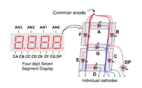
Each of the 4 digit displays have 7 leds that form a figure 8, and an 8th for a period in the lower right hand corner. As you can see in the diagram, all of the leds in the segment have their anodes connected, and each one has a different cathode connection. If you want to put a "1" on the display, you would want led B and C to turn on and everything else to turn off, so you drive the anode to 1, and the B and C cathodes to 0, so that current will flow through the B and C led, and it will light up. If you put a 1 on the cathodes of all the other leds, then the anode and cathode of those leds will be at the same potential, no current will flow, and it stays dark. Since there are 4 segment displays (4 sets of leds arranged in a figure 8 with a "period" LED in the lower right corner), to get each one to have the right pattern you would drive the common anode pin to 1, and the cathodes of the LEDS you want to light to 0, and the ones you want to stay dark drive with a 1. The way the led display is built is to have each of leds in each display have a common cathode with the corresponding LED in the other displays. For instance, leds A in the first segment display has its cathode tied to led A in the 2nd, 3rd, and 4th. And so on for the other LEDs in the segment.
The diagram below is on page 15 of the manual:
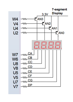
It shows that the way the anode signals work is that there's a pin for each of the 4 anodes, called "AN0", "AN1", "AN2", and "AN3". Driving each of these high in order will turn on that particular display, and setting the cathode signals "CA", "CB", "CC", "CD", "CE", "CF", "CG", and "DP" to determine what pattern (what number or letter) you want each particular segment to display. Note however that the BASYS3 board inverts the "AN" signals, so to turn on the 1st one, you drive "AN0" low and the rest high and so on for the other 3 displays.
We will define digit[3:0] as the output where digit[0] is "AN0" and etc for the other 4 bits. Then we define segment[6:0] as the 7 segments of each display ("CA", "CB", etc) in order determined by the constraints file such that "CA" is segment[0] and "CG" is segment[6], and dp as the period led. So the constraints file will look like this:
##
## 7 segment display
set_property PACKAGE_PIN W7 [get_ports {segment[0]} ]
set_property IOSTANDARD LVCMOS33 [get_ports {segment[0]} ]
set_property PACKAGE_PIN W6 [get_ports {segment[1]} ]
set_property IOSTANDARD LVCMOS33 [get_ports {segment[1]} ]
set_property PACKAGE_PIN U8 [get_ports {segment[2]} ]
set_property IOSTANDARD LVCMOS33 [get_ports {segment[2]} ]
set_property PACKAGE_PIN V8 [get_ports {segment[3]} ]
set_property IOSTANDARD LVCMOS33 [get_ports {segment[3]} ]
set_property PACKAGE_PIN U5 [get_ports {segment[4]} ]
set_property IOSTANDARD LVCMOS33 [get_ports {segment[4]} ]
set_property PACKAGE_PIN V5 [get_ports {segment[5]} ]
set_property IOSTANDARD LVCMOS33 [get_ports {segment[5]} ]
set_property PACKAGE_PIN U7 [get_ports {segment[6]} ]
set_property IOSTANDARD LVCMOS33 [get_ports {segment[6]} ]
##
## LED period (dot)
set_property PACKAGE_PIN V7 [get_ports dp]
set_property IOSTANDARD LVCMOS33 [get_ports dp]
##
## digit select
set_property PACKAGE_PIN U2 [get_ports digit[0] ]
set_property IOSTANDARD LVCMOS33 [get_ports digit[0] ]
set_property PACKAGE_PIN U4 [get_ports {digit[1]} ]
set_property IOSTANDARD LVCMOS33 [get_ports {digit[1]} ]
set_property PACKAGE_PIN V4 [get_ports {digit[2]} ]
set_property IOSTANDARD LVCMOS33 [get_ports {digit[2]} ]
set_property PACKAGE_PIN W4 [get_ports {digit[3]} ]
set_property IOSTANDARD LVCMOS33 [get_ports {digit[3]} ]
The way the verilog code works is to do the following:
To display 4 different numbers in the 4 different digits, what you have to do is to store the 4 numbers in registers, and then loop over the 4 digits, sending the stored number to the segments one at a time. This has to be done with the 4ms clock (MSB of the 18 bit counter) so that you don't see "flickering".
The following code can be used to chnage the 4-bit hex number of the 16 bit counter into the right combinations of segments to display the number. The inputs are a clock (used to clock data into registers so that it's in memory), a 4-bit number ("number[3:0]") and the corresdponding 7-bit segment pattern cooked up so that the numbers 0-9,A,B,C,D,E,F appear. This of course means that the displayed 4-digit number will be in hex. We will use parameters (as explained above) to define the 16 different patterns that will give us the digits 0-9,a-f, and a case statement that checks on the 4-digit number that we want to transform:
`timescale 1ns / 1ps
//////////////////////////////////////////////////////////////////////////////////
// Company:
// Engineer:
//
// Create Date: 08/15/2017 02:34:58 PM
// Design Name:
// Module Name: segnum
// Project Name:
// Target Devices:
// Tool Versions:
// Description:
//
// Dependencies:
//
// Revision:
// Revision 0.01 - File Created
// Additional Comments:
//
//////////////////////////////////////////////////////////////////////////////////
`timescale 1ns / 1ps

module segnum (
    input clk,
    input [3:0] number,
    output reg [6:0] seg = 0
    );

    parameter [6:0] p0 = 'b1000000;
    parameter [6:0] p1 = 'b1111001;
    parameter [6:0] p2 = 'b0100100;
    parameter [6:0] p3 = 'b0110000;
    parameter [6:0] p4 = 'b0011001;
    parameter [6:0] p5 = 'b0010010;
    parameter [6:0] p6 = 'b0000010;
    parameter [6:0] p7 = 'b1111000;
    parameter [6:0] p8 = 'b0000000;
    parameter [6:0] p9 = 'b0010000;
    parameter [6:0] pa = 'b0001000;
    parameter [6:0] pb = 'b0000011;
    parameter [6:0] pc = 'b1000110;
    parameter [6:0] pd = 'b0100001;
    parameter [6:0] pe = 'b0000110;
    parameter [6:0] pf = 'b0001110;

    always @ (posedge clk)
        case (number)
            'h0: seg <= p0;
            'h1: seg <= p1;
            'h2: seg <= p2;
            'h3: seg <= p3;
            'h4: seg <= p4;
            'h5: seg <= p5;
            'h6: seg <= p6;
            'h7: seg <= p7;
            'h8: seg <= p8;
            'h9: seg <= p9;
            'hA: seg <= pa;
            'hB: seg <= pb;
            'hC: seg <= pc;
            'hD: seg <= pd;
            'hE: seg <= pe;
            'hF: seg <= pf;
        endcase


endmodule
Now we need a circuit that will input a 4-digit hex number (number[15:0]), and with a clock loop over the 4 digits, sending each of the 4 digits to the segments one at a time. The module name here will be called display4.v, and will have the following IO ports:
module display4(
    input clk100,
    output reg [3:0] digit = 0,  //digit 3 is leftmost (MSD), digit 1 is rightmost (LSD)
    output reg [6:0] segments = 'b111111, //7 segments: top,mid,bot and top_left/bot_left and same for right
    output reg period,
    input [15:0] number     //4 hex digits
    );
We associate the 4-bit digit with the 16-bit number like this:
wire [3:0] digit3 = number[15:12];
wire [3:0] digit2 = number[11:8];
wire [3:0] digit1 = number[7:4];
wire [3:0] digit0 = number[3:0];
Next we make a clock from the 100MHz input clock that will refresh at a high enough rate so that there's no flickering. 60Hz means a 16ms period. If we start with a 10ns period, then we need around $10^6$ ticks of the 100MHz clock for each refresh, which means a counter that's around 20 bits. So we can make a 19 bit counter and use the MSB, and that will be at least 16ms (it will be around 5ms, which means more like 200Hz refresh will be just fine). However, due to the fact that we can only send 1 of 4 digits at a time, and we have to cycle through, we need to run this slower clock 4x faster. So we will make an 18-bit counter, and use bit 17 (starting from 0) as the clock, and increment a 2-bit register for the digit pointer. The code will look something like this:
reg [17:0] counter = 0;
always @ (posedge clk100) counter <= counter + 1;
wire digit_clock = counter[17];
reg [1:0] which_digit;
always @ (posedge digit_clock) which_digit <= which_digit + 1;
Putting it all together, we make a case statement inside an always block using digit_clock as the posedge trigger, use segnum to set the segment display, and loop. The full code for display4.v looks like this:
`timescale 1ns / 1ps
//////////////////////////////////////////////////////////////////////////////////
// Company:
// Engineer:
//
// Create Date: 08/14/2017 04:14:07 PM
// Design Name:
// Module Name: counter
// Project Name:
// Target Devices:
// Tool Versions:
// Description:
//
// Dependencies:
//
// Revision:
// Revision 0.01 - File Created
// Additional Comments:
//
//////////////////////////////////////////////////////////////////////////////////
`timescale 1ns / 1ps


module display4(
    input clk100,
    output reg [3:0] digit = 0,  //digit 3 is leftmost (MSD), digit 1 is rightmost (LSD)
    output reg [6:0] segments = 'b111111, //7 segments: top,mid,bot and top_left/bot_left and same for right
    output reg period,
    input [15:0] number     //4 hex digits
    );


//
// well, verilog arithmetic is pretty good so let's just let it figure out the digits
//
wire [3:0] digit3 = number[15:12];
wire [3:0] digit2 = number[11:8];
wire [3:0] digit1 = number[7:4];
wire [3:0] digit0 = number[3:0];

//
// make a clock from the 100MHz clock that refreshes at around 60Hz or more.
// that means a period of at least 16ms.   with a 10ns period input clock,
// if you set up a register with N bits, the period is given by:
// T = 10ns * 2^{N+1}
// so we want 16ms = 10ns * 2^{N+1} solving for that gives 19.6 bits so we use 19
// to make it a little faster than 60Hz.
//
// But, since we can only have one digit on at a time, we need to change the digits
// by 4 times this value.   that means we need to run the clock 4x faster, and use
// that slow clock to increment a 2-bit pointer and cycle through the 4 digits one at a time
//
reg [17:0] counter = 0;
//
// use negedge so we don't have race conditions later
//
always @ (negedge clk100) counter <= counter + 1;
wire digit_clock = counter[17];
reg [1:0] which_digit;
always @ (posedge digit_clock) which_digit <= which_digit + 1;

wire [6:0] wseg0, wseg1, wseg2, wseg3;
segnum S0 ( .clk(clk100), .number(digit0), .seg(wseg0) );
segnum S1 ( .clk(clk100), .number(digit1), .seg(wseg1) );
segnum S2 ( .clk(clk100), .number(digit2), .seg(wseg2) );
segnum S3 ( .clk(clk100), .number(digit3), .seg(wseg3) );

always @ (posedge digit_clock) begin
    period <= 1;       // turn it off for now
    case (which_digit)
        'h0: begin
                digit <= 'b1110;
                segments <= wseg0;
            end
        'h1: begin
                digit <= 'b1101;
                segments <= wseg1;
            end
        'h2: begin
                digit <= 'b1011;
                segments <= wseg2;
            end
        'h3: begin
                digit <= 'b0111;
                segments <= wseg3;
            end
      endcase
end

endmodule
Now that we have the display code all defined, we can instantiate the display4 circuit, and remember to have both display4.v and segnum.v in your project:
    display4 LED_DISPLAY (
        .clk100(clk),
        .number(the_count),
        .digit(digit),
        .segments(segment),
        .period(dp));
The following are the xdc constraints for this project, including all of the other things needed:
## clock
set_property PACKAGE_PIN W5 [get_ports clk]
set_property IOSTANDARD LVCMOS33 [get_ports clk]
##
## 16 LEDs
set_property PACKAGE_PIN L1 [get_ports {LED[15]}]
set_property IOSTANDARD LVCMOS33 [get_ports {LED[15]}]
set_property PACKAGE_PIN P1 [get_ports {LED[14]}]
set_property IOSTANDARD LVCMOS33 [get_ports {LED[14]}]
set_property PACKAGE_PIN N3 [get_ports {LED[13]}]
set_property IOSTANDARD LVCMOS33 [get_ports {LED[13]}]
set_property PACKAGE_PIN P3 [get_ports {LED[12]}]
set_property IOSTANDARD LVCMOS33 [get_ports {LED[12]}]
set_property PACKAGE_PIN U3 [get_ports {LED[11]}]
set_property IOSTANDARD LVCMOS33 [get_ports {LED[11]}]
set_property PACKAGE_PIN W3 [get_ports {LED[10]}]
set_property IOSTANDARD LVCMOS33 [get_ports {LED[10]}]
set_property PACKAGE_PIN V3 [get_ports {LED[9]}]
set_property IOSTANDARD LVCMOS33 [get_ports {LED[9]}]
set_property PACKAGE_PIN V13 [get_ports {LED[8]}]
set_property IOSTANDARD LVCMOS33 [get_ports {LED[8]}]
set_property PACKAGE_PIN V14 [get_ports {LED[7]}]
set_property IOSTANDARD LVCMOS33 [get_ports {LED[7]}]
set_property PACKAGE_PIN U14 [get_ports {LED[6]}]
set_property IOSTANDARD LVCMOS33 [get_ports {LED[6]}]
set_property PACKAGE_PIN U15 [get_ports {LED[5]}]
set_property IOSTANDARD LVCMOS33 [get_ports {LED[5]}]
set_property PACKAGE_PIN W18 [get_ports {LED[4]}]
set_property IOSTANDARD LVCMOS33 [get_ports {LED[4]}]
set_property PACKAGE_PIN V19 [get_ports {LED[3]}]
set_property IOSTANDARD LVCMOS33 [get_ports {LED[3]}]
set_property PACKAGE_PIN U19 [get_ports {LED[2]}]
set_property IOSTANDARD LVCMOS33 [get_ports {LED[2]}]
set_property PACKAGE_PIN E19 [get_ports {LED[1]}]
set_property IOSTANDARD LVCMOS33 [get_ports {LED[1]}]
set_property PACKAGE_PIN U16 [get_ports {LED[0]}]
set_property IOSTANDARD LVCMOS33 [get_ports {LED[0]}]
##
## buttons
set_property PACKAGE_PIN T18 [get_ports reset]
set_property IOSTANDARD LVCMOS33 [get_ports reset]
set_property PACKAGE_PIN U17 [get_ports btnCnt]
set_property IOSTANDARD LVCMOS33 [get_ports btnCnt]
##
## 7 segment display
set_property PACKAGE_PIN W7 [get_ports {segment[0]} ]
set_property IOSTANDARD LVCMOS33 [get_ports {segment[0]} ]
set_property PACKAGE_PIN W6 [get_ports {segment[1]} ]
set_property IOSTANDARD LVCMOS33 [get_ports {segment[1]} ]
set_property PACKAGE_PIN U8 [get_ports {segment[2]} ]
set_property IOSTANDARD LVCMOS33 [get_ports {segment[2]} ]
set_property PACKAGE_PIN V8 [get_ports {segment[3]} ]
set_property IOSTANDARD LVCMOS33 [get_ports {segment[3]} ]
set_property PACKAGE_PIN U5 [get_ports {segment[4]} ]
set_property IOSTANDARD LVCMOS33 [get_ports {segment[4]} ]
set_property PACKAGE_PIN V5 [get_ports {segment[5]} ]
set_property IOSTANDARD LVCMOS33 [get_ports {segment[5]} ]
set_property PACKAGE_PIN U7 [get_ports {segment[6]} ]
set_property IOSTANDARD LVCMOS33 [get_ports {segment[6]} ]
##
## LED period (dot)
set_property PACKAGE_PIN V7 [get_ports dp]
set_property IOSTANDARD LVCMOS33 [get_ports dp]
##
## digit select
set_property PACKAGE_PIN U2 [get_ports digit[0] ]
set_property IOSTANDARD LVCMOS33 [get_ports digit[0] ]
set_property PACKAGE_PIN U4 [get_ports {digit[1]} ]
set_property IOSTANDARD LVCMOS33 [get_ports {digit[1]} ]
set_property PACKAGE_PIN V4 [get_ports {digit[2]} ]
set_property IOSTANDARD LVCMOS33 [get_ports {digit[2]} ]
set_property PACKAGE_PIN W4 [get_ports {digit[3]} ]
set_property IOSTANDARD LVCMOS33 [get_ports {digit[3]} ]
Now we are ready to put all the code together into a single TOP.v. It should look something like this:
`timescale 1ns/1ps
//
module top(
    input clk, reset, btnCnt,
    output [15:0] LED,
    output [6:0] segment,
    output dp,
    output [3:0] digit);

    //
    //  debounce the btnCnt signal
    //
    wire btnCnt_level, btnCnt_1s;
    debouncer DEBOUNCE_COUNT(
        .clock(clk), .button(btnCnt), .level(btnCnt_level), .pulse(btnCnt_1s) );
    wire version_level, version_1s;
    //
    //  count button pushes
    //
    reg [15:0] the_count;
    always @ (posedge btnCnt_1s)
        if (reset) the_count <= 0;
        else the_count <= the_count + 1;
    assign LED = the_count;
    //
    //  display the count on the LED display and in the LEDs
    //
    display4 LED_DISPLAY (
        .clk100(clk),
        .number(the_count),
        .digit(digit),
        .segments(segment),
        .period(dp));
endmodule
To program the FPGA, follow the same procedure as detailed above.
The above project archive can be found here.