Creating a new project
When you run Vivado, you should see the following screen: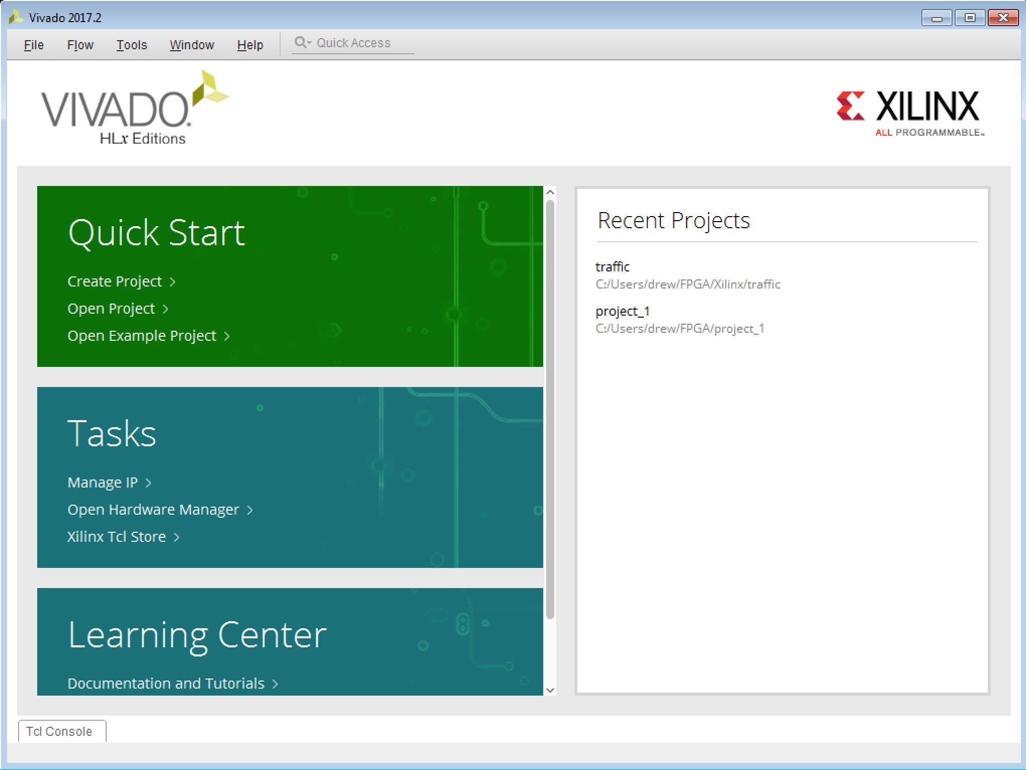
The next screen is called "Project Type". Click on the 1st radio button labeled "RTL Project", and hit "Next".
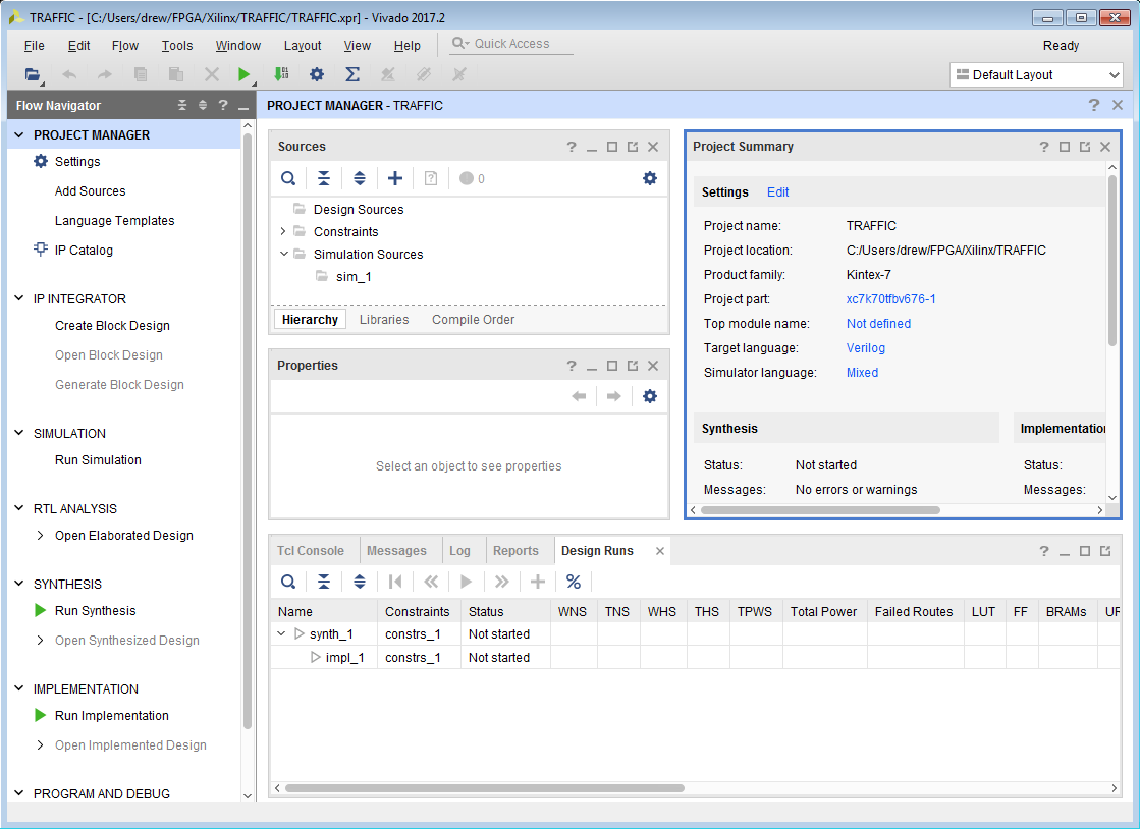
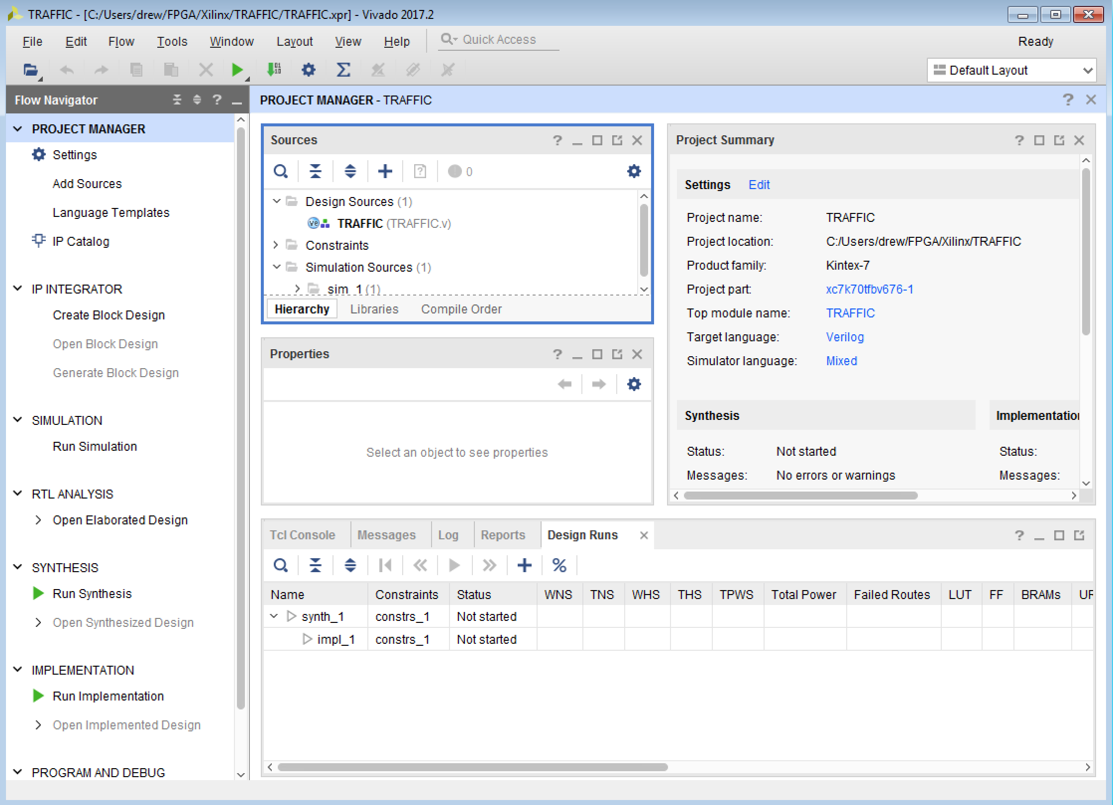
Next you will go to "Default Part". This is for people who know the part name of the FPGA they will be programming. In this case, we don't really care about the actual FPGA, so just it "Next" without specifying anything. That takes you to the final window where you can hit "Finish". You should now be at a window that looks like this:
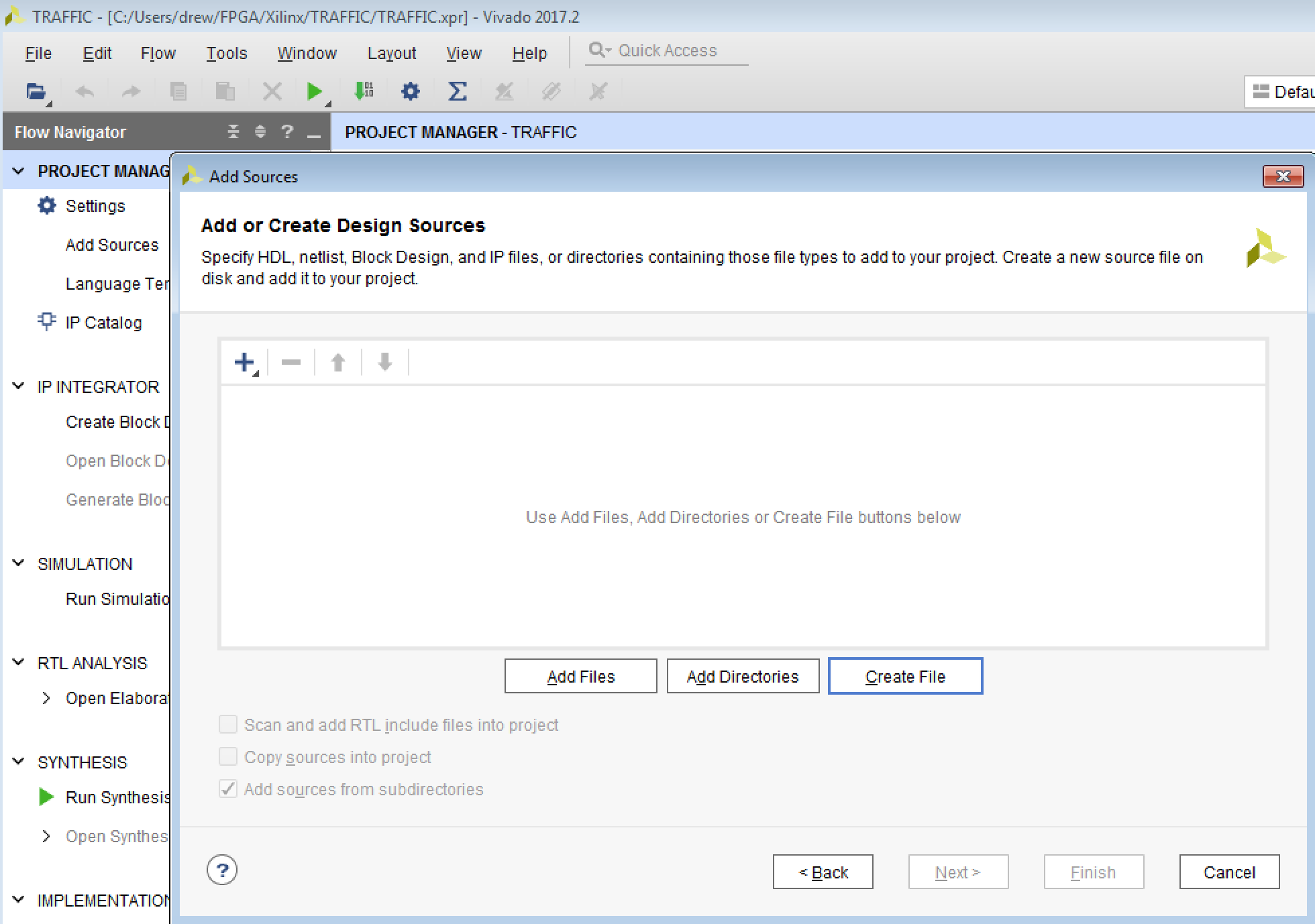
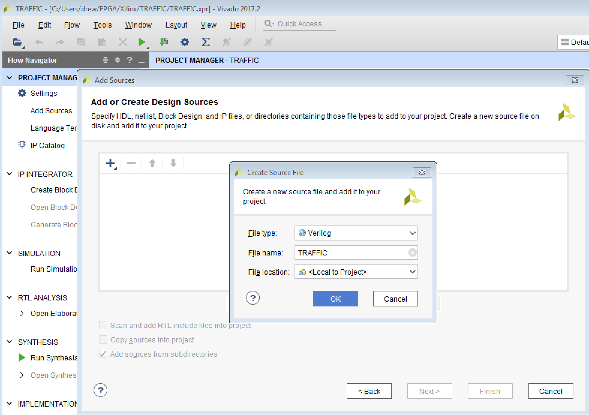
Now we need to add some source code. If you mouse over the "+" sign in the "Sources" subwindow, it should say "Add Sources (Alt+S)". Click there to bring up the "Add Sources" window. Make sure that "Add or create design sources" is set, and hit "Next". This brings up a window called "Add or Create Design Sources". Since you don't have any sources, you want to click on the box called "Create File", as seen below:
The Vivado window should now look like this:
Traffic light Verilog code
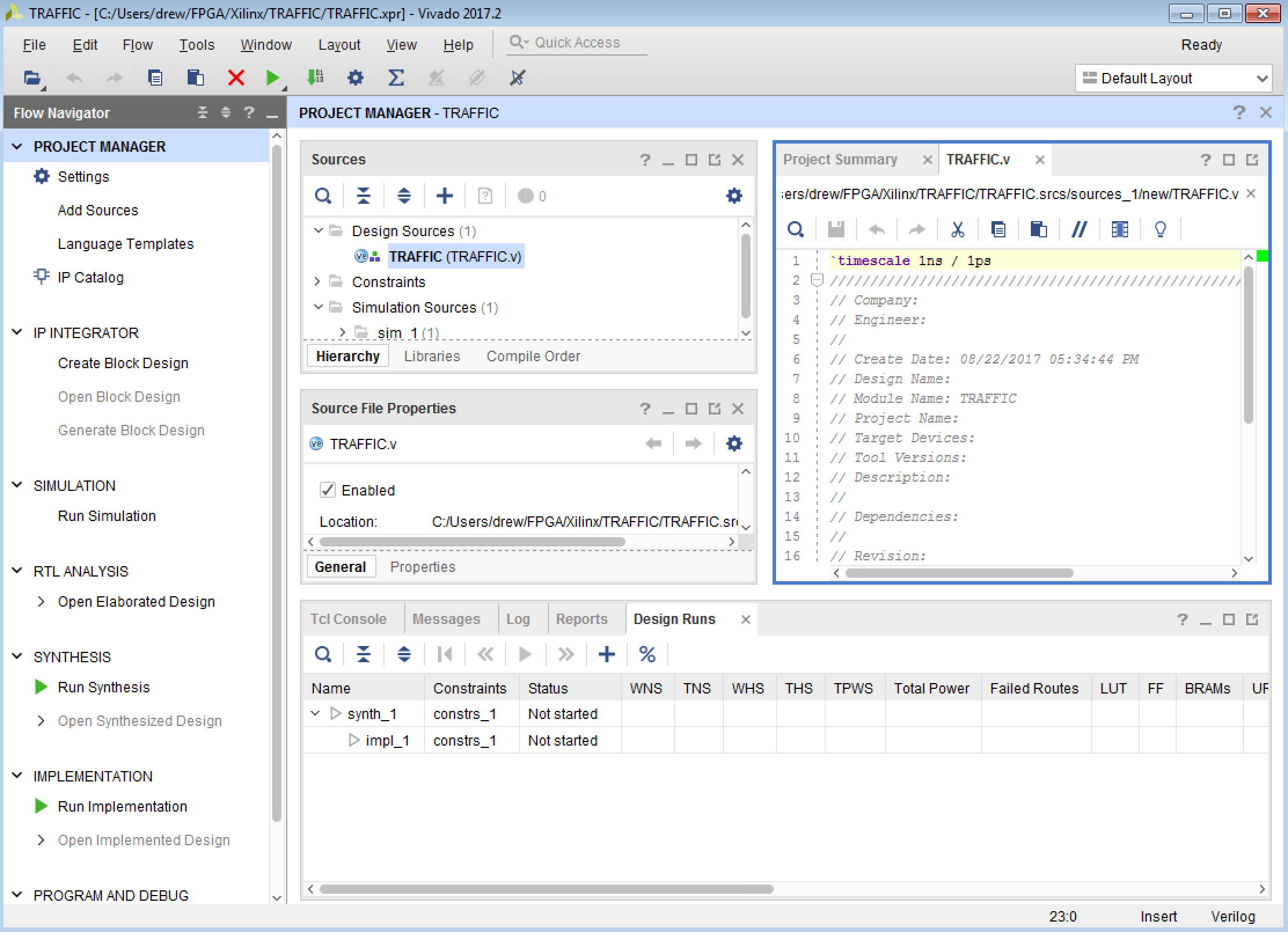
Next we have to enter the code into TRAFFIC.v, by double clicking on that name. It brings up an editable subwindow to the right that looks like this:
The top line of TRAFFIC.v has the following line of code:
`timescale 1ns / 1psIn Verilog, the backwards apostrophy "`" denotes a "directive", used for things like include files, etc. The "timescale" directive is used to denote the time scale for the simulation, and the precision. The timescale here is 1ns (the "precision" is 1ps), and the way that is used is that in the stimulus, if you want to specify a delay, then if you say "#22" then that means 22ns. The precision is for the simulator and represents the smallest time you can see on the waveform. 1ps is pretty precise, and unless you know that you can simulate things to that level, you should probably change the precision to 1ns just to save simulation time. But you can also leave the timescale at "1ns/1ps" and all will be well.
We are ready now to code up the finite state machine (FSM) for the traffic light.
The circuit will have 3 inputs (clock, enable, and reset) and 3 outputs
(the red, green, and yellow lights). So the first few verilog lines
will look like this:
For this project, we will need an externally provided clock input, so let's use
the 100MHz clock (10ns period) that is already on the BASYS3 board.
Now, let's set the time for the lights to be
10s for green, 10s for red, and 2s for yellow (use 10s so that you don't have to
wait too long to see it change on the FPGA). That means we need to wait
$10s/10^{-8}s=10^9$ ticks of the clock for the green and red light, and
1/5 that number for the yellow. If $2^10\sim 1000$, then to get to $10^9$
we will need $2^7$ (137) times $2^20\sim 10^6$ ticks, which means we need a
30-bit counter to get to $10^9. In fact we need 3 of them, but let's use
even bigger counters so that we can accommodate 30s for the reg and green.
The code looks like this:
Note that the reset condition here is a "synchronous reset", that is when the reset
line is asserted, the counters won't reset until the next rising edge of the system
clock. You could easily make an "asynchronous reset" by doing this:
Also, we only count when the enable line is asserted. This means enable is a
level, not a pulse!
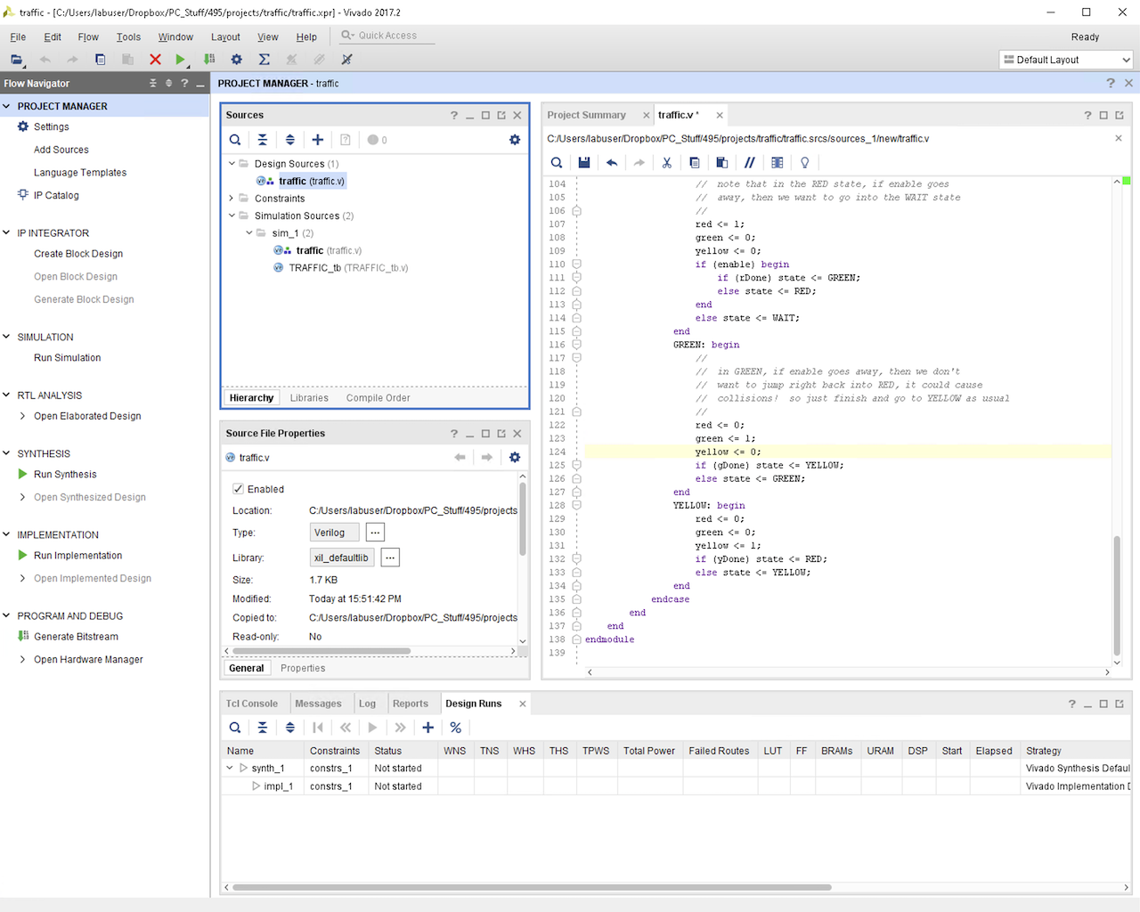
Next we implement the state machine that will control which light is on, and in
what order. We will have 4 states: WAIT, to wait for enable, and a state for
each of the different lights (RED, GREEN, YELLOW). That's 4 states, which we
can implement with a 2-bit parameter for the state and a 2-bit state register
to hold the state value:
Make sure your code is set and that there are no errors (you can see errors, the
Verilog editor will show you some squiggly lines).
Assuming there are no typo's, you should be ready to simulate
the FSM.
Before you take any Verilog code you've written and run it in an FPGA, you
should always run a simulation and look at waveforms. This is really
important for any successful programmable logic project, because as we know
form Murphy's law, nothing ever works correctly the first time.
We will simulate the traffic code using the standard tool that comes in the
development tool from Xilinx. But first, we
have to write our own "stimulus". That means we need to write some
Verilog that controls the inputs to our circuit ("TRAFFIC"), and checks on
the outputs, and presents them in a viewable waveform. There are tools
that allow you to generate stimulus using waveforms directly (pointing and
clicking), however it's much more powerful to use Verilog directly, and
the bottom line is that a simulation is only as good as the ability to
faithfully represent the inputs.
To generate the testbench, we first generate a new source file that
will be plugged into the project. In the same "Sources" subwindow
that you used create the TRAFFIC.v source, click again on the "+"
button to bring up the "Add Sources" window. This time click on the
3rd choice, "Add or create simulation sources",
and click "Next". The brings up the "Add or Create Simultion Sources"
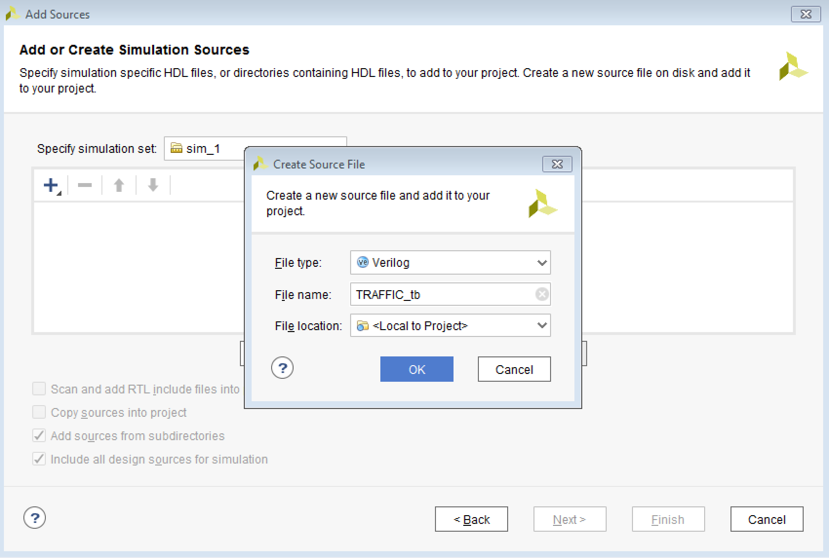
window, where you click "Create File", which brings up a "Create Source File"
window where you can name the new source. Let's call it "TRAFFIC_tb"
("tb" for "testbench") and it OK. It should look like this before you
hit OK:
Hit OK and "Finish", and "OK" at the next "Define Module" window, and
confirm "Yes". Vivado should look like this now:
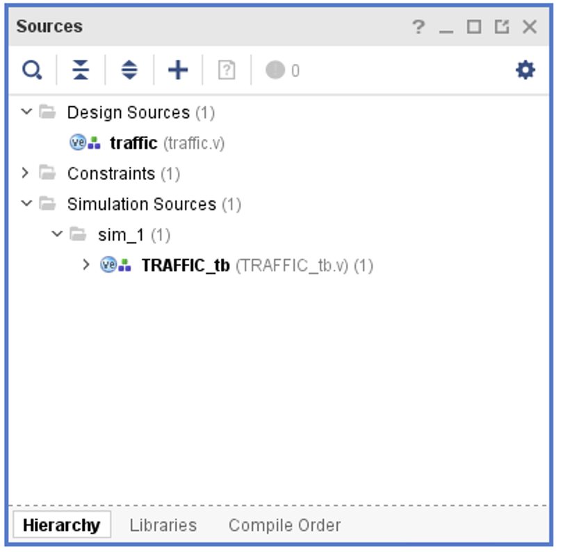
Next we have to edit TRAFFIC_tb.v to add the stimulus. To do this,
click on the ">" symbol on the line "sim_1". It should then show
you 2 files: TRAFFIC.v under "Design Sources"
and TRAFFIC_tb.v under "Simulation Sources". The latter is what will
use to stimulate the former.
If all is well you should see the correct hierarchy like in
the following, with "traffic.v" (or whatever you named it) underneath "TRAFFIC_tb.v".
Double click on TRAFFIC_tb.v and it will create
a new tab in the subwindow to the right. That window should be
empty except for the timescale directive, some comments, and
the module declaration. Now we learn how to write Verilog stimulus code.
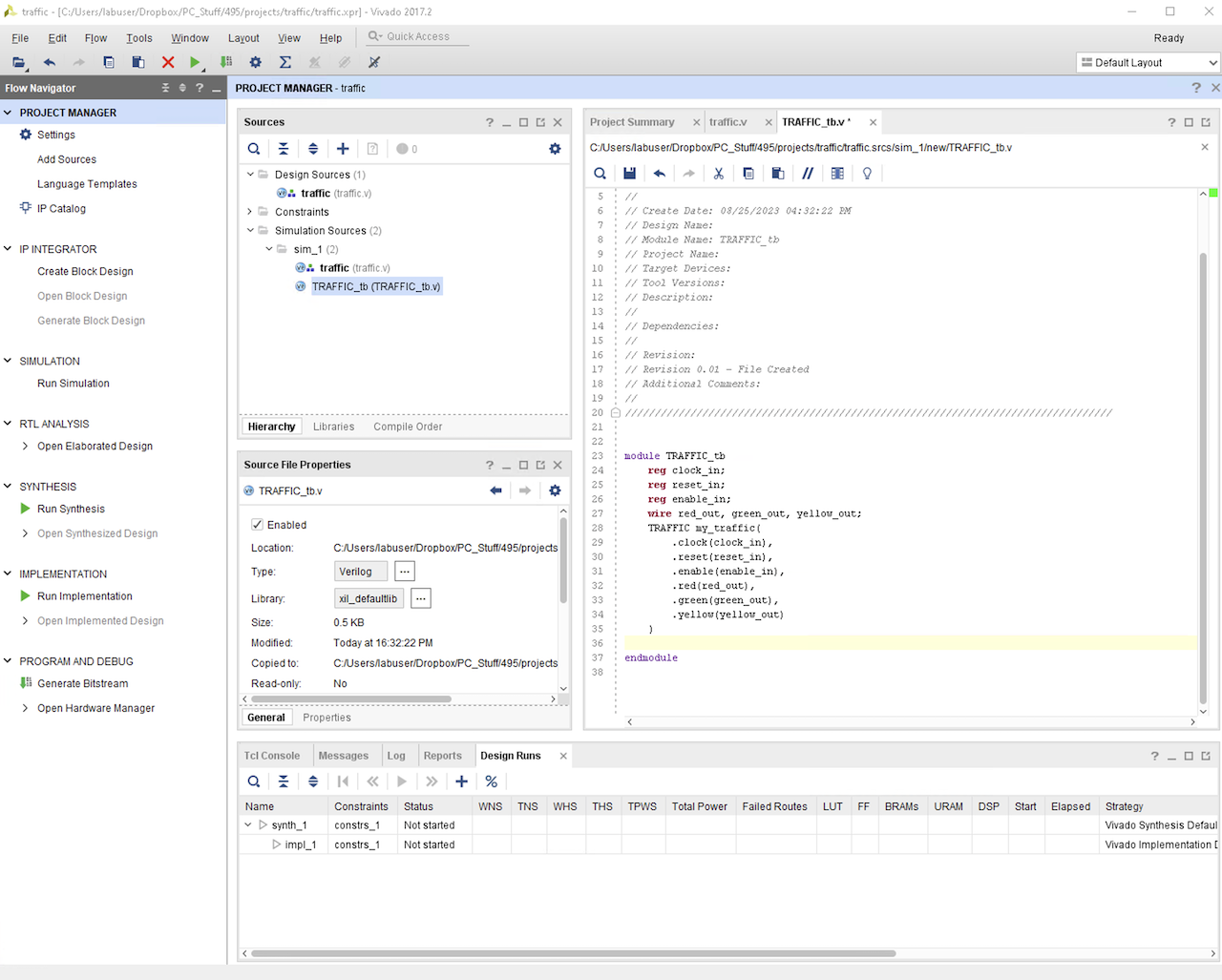
The first thing we want to do is to instantiate the TRAFFIC.v circuit,
and define the inputs that go
into TRAFFIC.v, so that we can stimulate them, and the outputs,
so we can see how they behave. We do this with the following code:
Paste that code into the file, and
if there are no typo's, it should look like this:
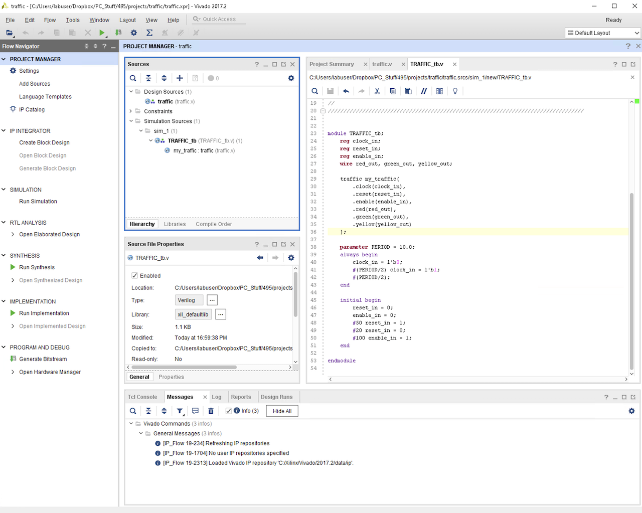
Next we want to specify the enable and
reset lines, which is done in the following
code:
When you save this code, if there are no typos, then Vivado should recognize
that you are instantiating "traffic" inside TRAFFIC_tb, and this will be reflected
in the hierarchy of modules (click on the right carot next to TRAFFIC_tb), showing
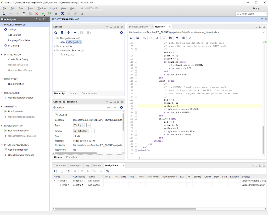
TRAFFIC_tb.v and traffic.v underneath it:
Now we are ready to run the simulation. In the left pane of the Vivado
window, you should see "Run Simulation". Click on it and you should see
a pop-up window. Click on the top line, "Run Behavioral Simulation".
What that means is the following: the verilog code for
TRAFFIC.v has no timing information (it's actually possible to add it,
but that's another story). So when AND and OR gates change state, and
DFFs see posedges, they happen "instantly". As such, the waveforms will show
the behavior of the logic, but won't tell you anything about actual timing.
Doing that is possible, but only after you've actually run the full
synthesis and implementation. I have found that most of the bugs are
found right away by doing a behavioral simulation. If you have timing
problems (so-called race conditions) then you probably won't see them in
any kind of simulation easily, you just have to run the thing in an FPGA
and do a first order checking there for mistakes before a real timing
simulation. Also, the timing simulation uses best guesses for the actual
delays inside the FPGA. And each FPGA is slightly different. Best to
find errors in situ first!
If you have any errors, the system will report it. On the bottom, you
will see a panel with 5 tabs labelled "Tcl Console", "Messages", "Log",
"Reports", and "Design Runs". You will have to wade through these to
figure out what the errors are, but usually it's just syntax. The
"Tcl Console" should tell you the exact errors.
Assuming all goes well, you should now be looking at the following
rather large window:
The default scope is "TRAFFIC_tb", so you can see in the waveform window
all of the signals present in that source. You won't see anything
interesting yet, because the simulation defaults are not set correctly.
Notice on the top line of the window the usual tabs "File", "Edit", etc.
Towards the end, you will "Quick Access".
Below the Quick Access menu name are 3 icons, then
a text window that says "100", then one that says "us", then some other
icons. The first of the 3 is the "Restart" icon, for restarting the
simulation. The next one, a triangle, is "Run All" (run), and the 3rd
is a triangle with a little "m" below it, which means run for a time
period as specified in the next 2 windows, which means 100us. And
that means the simulation has run for 100us (100 microseconds).
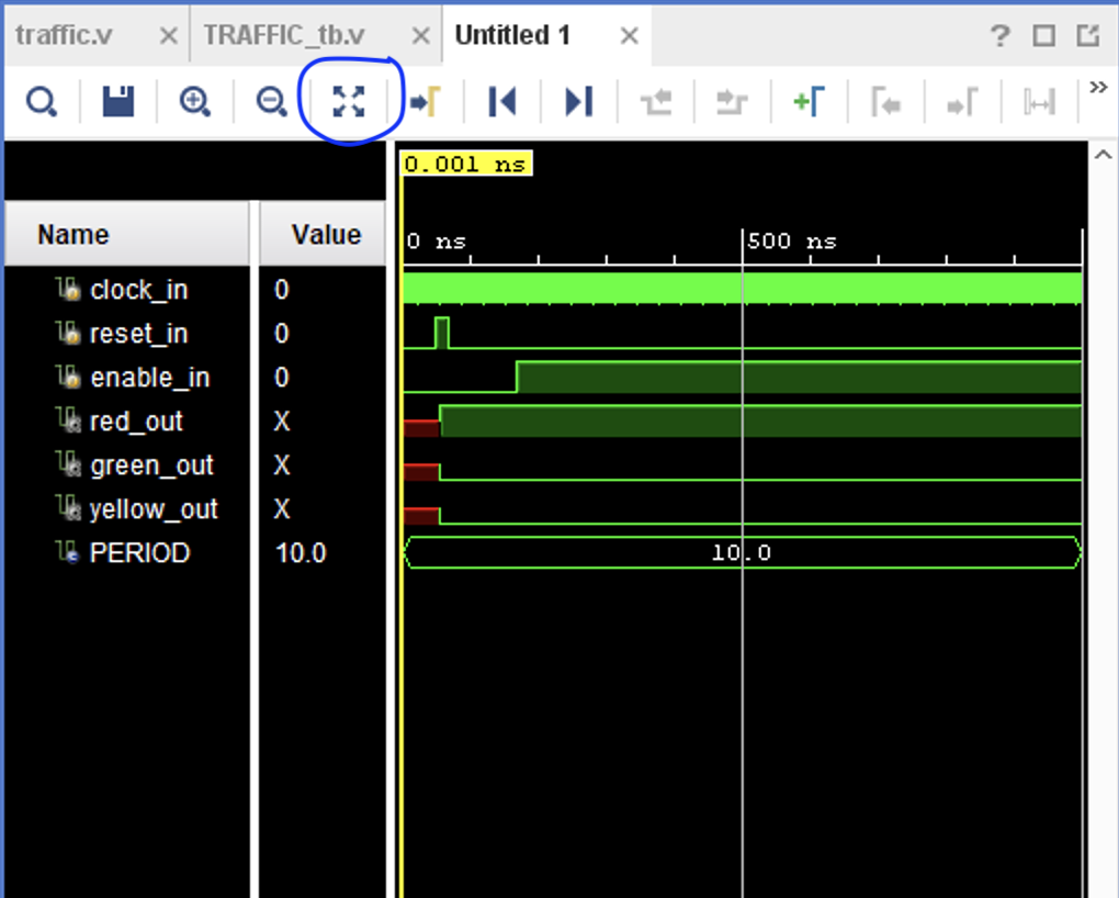
That's enough time to see the initial reset and enable. So in
the waveform window (black background) on the right, click on
the icon that has 4 arrows pointing outwards from the center, that
will set the waveform window so that you can see the first 100us
nicely. It should look like this (I've outlined that particular icon
in blue):
The thick yellow line next to "clock_in" is thick because it's showing
the clock, which is changing every 10ns but the window scale is set
to 100us, which is 10,000 clock ticks You can see the reset line go
high for a few cycles, then the enable_in line goes high. The
red_out, green_out, and yellow_out signals are the same as the
red, green, and yellow outputs of traffic.v, and once the reset
line is asserted, those 3 *_out signals change from a red level
to either 0 or 1. That's because before the reset is asserted,
these signals are undefined in traffic.v. If we didn't have
the reset, the simulation would show those signals stuck at some
undetermined value (hence the "X" under the "Value" column).
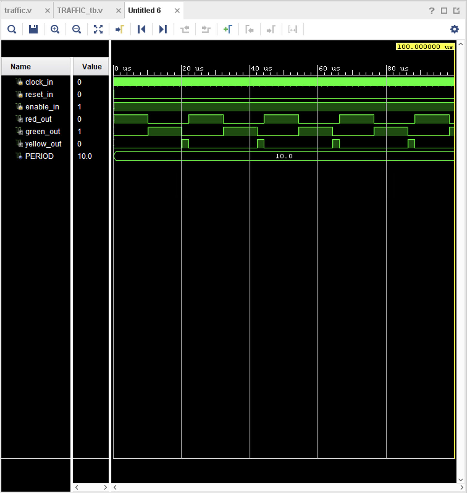
Now we want to see all of the lights change.
But it's going to take forever because the precision is 1ps,
and because the timers are counting up to 100million or so!
So let's try canceling the simulation, and close the window and
go back to the source code and change the precision to 1ns instead
of 1ps in both files. And to make things very easy, let's change
the timers so that they go off instead of 10s and 2s, let's do
10us and 2us to make things faster. So go into traffic.v and change
the yDone, gDone, and rDone lines to something like this:
Now, rerun the simulation, and put 100 and us in the simulation windows
and hit the start button. Then hit the expand button and you should
see this:
In this project, we have 3 inputs (clock, reset, enable) and 3 outputs
(red, green, yellow lights). We are going to download this project into
the FPGA, and connect these to the gadgets on the BASYS3 board.
So we will need to know what FPGA input pin the clock comes in on,
and how to connect the reset button to one of the BASYS3 push buttons,
and the enable to one of the BASYS3 switches. This is quite easy, as all
of this information is in the user manual, which you can get directly from
Digilent
here, or just grab it directly from
here.
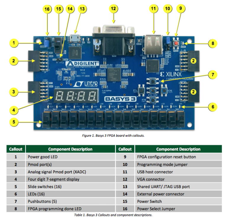
The top of the reference manual gives an overview, then shows a picture
of the board, and so on. More importantly, on page 2 you will see the
following:
which shows all of the gadgets on the board.
Each one of the "Callouts" is described in a section of the reference
manual below that picture. So all you need to do is find the description.
For instance, if you search for "clock", you will find on page 6, section
"4 Oscillators/Clocks" the following first sentence:
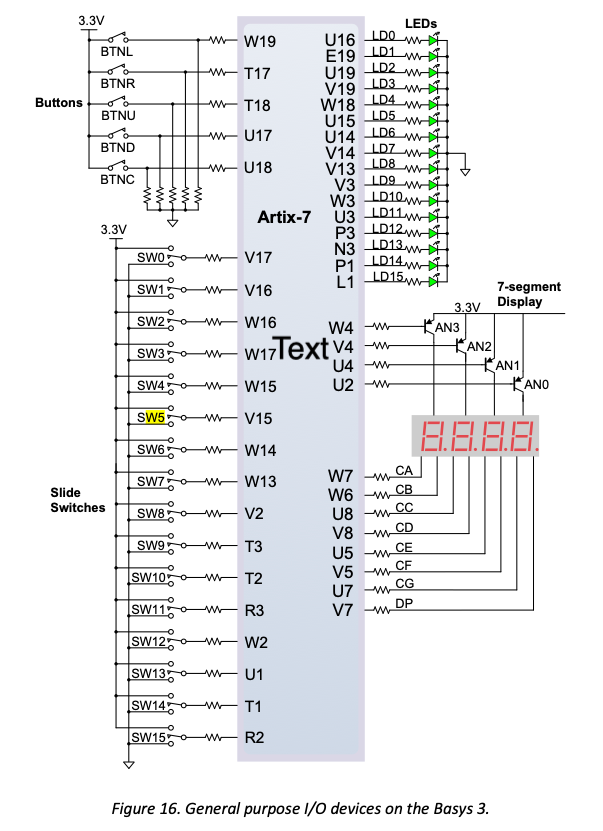
The 2 other inputs, enable and reset, come from a switch and a button.
On page 15 of the manual, under section "8 Basic I/O", you will see the
following schematic:
This is all you need to know to finish the connections! Let's use
the center button of the BASYS3 board (labeled BTNC) for the reset.
On the schematic above, you can see that BTNC is connected to pin U18
on the FPGA ("Artix-7"). For the enable line, let's use the first
(lowest) switch, labeled "SW0", which is connected to pin V17.
For the reg, green, and yellow lines, let's use the 1st 3 LEDs, which
are labeled "LD0", "LD1", and "LD2", connected to pins U16, E19, and
U19. So our verilog/FPGA connections will be:
The connections are made inside a new file in Vivado called a "constraints"
file (there are lots of various constraints, and specifying pins is one of
them). To make this file, make sure the simulation window is gone (click on
the X, upper right), and go to the "Sources" window, and click on the "+"
sign. It will bring up a "Add Sources" popup, with 3 choices. Choose
the top one "Add or create constraints" and hit Next. Then click on
"Create File" and type a name (maybe same as your top level Verilog
source file name) in the "File name:" field, and hit OK. Then hit Finish.
If you look at the Sources window, you should now see the following
(note where it says "> Constraints (1)"):
Click on the carot and open it up, and you should see "constrs_1 (1)"
and under that the name of your constraints file (mine is "traffic.xdc").
The xdc type means a Xilinc constraints file. Double click on that and
it will pop into the editor window to the right.
Here's what you have to type for each constraint (and I'll use the clock
for example):
Now do the same thing for all of the 5 other pin/port combinations.
Your file should look like this:
Once you have saved the xdc file, you are ready for the next step
called "SYNTHESIS"
Note that the Vivado synthesizer is pretty good, but there are standalone
synthesizers that people have built (into companies) that you can buy
(and they are quite expensive although there might be university discounts),
and they are also a lot better, at least potentially. "Better" means that
if you have an FPGA with a finite number of resources (gates, DFF, memory,
etc) and you find that the project you want to implement won't fit (you
are using too many resources), then you can try one of these other
synthesizers, and sometimes these actually can find a way to implement
things in a much smaller "area" (area means number of logic cells inside the
FPGA).
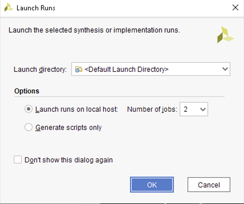
To run the Synthesizer, click on "SYNTHESIS" in the Flow Navigator. It
then brings up a "Launch Runs" window like this:
You can just click "OK". You might also click "Don't show this dialog again"
so you don't have to click "OK" every time you run the systhesis.
The synthsizer will run, and you can see "Running synth_design" and a progress
wheel at the upper right corner of Vivado.
If you have any errors, you will see them in the "Messages" and "Log" window
at the bottom of Vivado. If there are errors, you have to fix them and rerun.
If there are no errors, you will see a "Synthesis Completed" pop-up window.
It will tell you that "Synthesis successfully completed" and ask if you want
to go to the next step, which is IMPLEMENTATION. You can hit Cancel to
just stop there, or you can click the "View Reports" radio button and hit OK,
that will show you all kinds of interesting things about your design.
The report will show up in the "Reports" tab in the window at the bottom of
Vivado. Sometimes that report is useful if you want to see details about
the resources.
The implementation stage is where the Vivado program uses the result of
the synthesis, which takes the logic from the Verilog program and turns it
into a "netlist", which tells the system what resources are needed and
how they are connected.
It then does what it needs to do to be able to download something into
the FPGA to make it work. It is also the stage where it takes any
constraints you might have (for instance, a constraint that specifieds
the maximum time it can take for a signal to get from one DFF to another,
etc) and implements the constraints.
Click on "Run Implementation". You will see a progress wheel, upper right
corner of Vivado, and it will tell you what it's doing (e.g. "Initializing",
or "Running route_design", etc). If it finishes ok, you will get a
"Implementation Completed" popup, and it will ask you if you want to
"Open Implemented Design", "Generate Bitstream", or "View Reports".
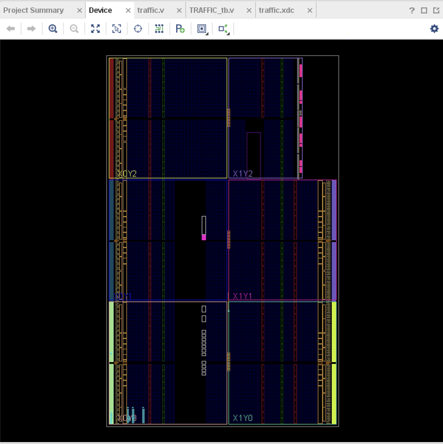
Assuming that the implementation worked ok, you can "Open Impelmented Design"
but it will take awhile, and come up with a very nice graphical display
of how the design fits inside the FPGA. It will look like this:
It's impressive, but unless you want to fiddle around with where Vivado
placed anything, then it's not very useful. And I've never had to play
such a fiddle!
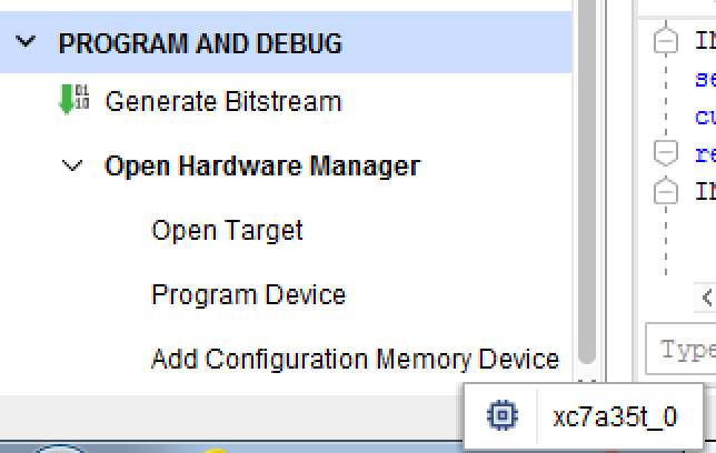
Next is to generate the bitstream file that goes into the FPGA.
Under "PROGRAM AND DEBUG" click on "Generate Bitstream". This can be
fast or slow depending on how big the project is. Once finishes it will
open up a "Bitstream Generation Completed" popup and ask if you want to
go ot the next step, which is to download to the device ("Open Hardware
Manager"). You can either open the hardware manager, or click cancel
and open it clicking to expand "Open Hardware Manager" under
"Generate Bitstream".
You have to set up the BASYS3 board correctly for our projects here, and
it has some options so let's make sure everything is set up so that we can
download code into the FPGA over the USB port. To do this, take a look
at this overview of the board:
The power on switch is labeled 15. We want to make sure that the
board is powered by the USB and not an external 5V powersupply. To do this,
look at item 16, the "Power Select Jumper". Make sure that the blue jumper
is set to "USB" (bottom 2 pins connected). Then make sure that item 10,
the "Programming mode jumper", is set to the top 2 pins, labeled "SPI".
That allows you to program the flash over USB.
That's it. When you power up the board, it will automatically load the
program in flash. You can override this by programming directly into
the FPGA memory (bit file, see below) or programming the flash directly
and then letting the FPGA take it's program from flash.
What Vivado does when you install it is to install drivers to download
into the FPGA over USB. When you right click on "Open Hardware Manager"
you will see "Open Target", "Program Device", and "Add Configuration Memory
Device". The 1st one will be selectable but the next 2 will be grayed out
the first time you do this. If you click on Open Target, you should see
the option "Auto Connect". It will then scan the drivers to see if the
USB driver is there, and if the FPGA BASYS3 board is connected and powered
up (and configured correctly for USB downloading and power). If you've
done that part ok, then click on "Auto Connect", it should show a
"Connecting to Server" (which is just another program running that
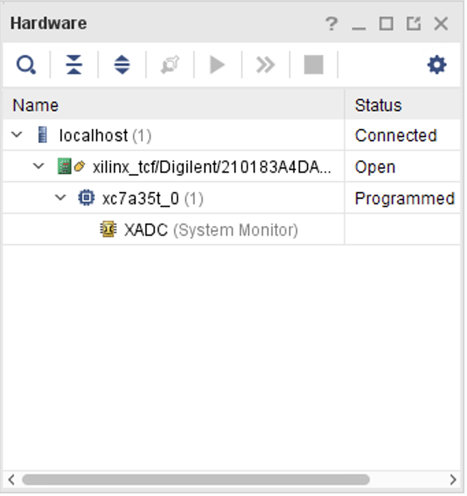
connects Vivado to the drivers). A new window will now open inside
Vivado where the old "Sources" window used to be and will look like this:
What you see in the hierarchy is the localhost (your PC), then the
Digilent board, then the FPGA ("xc7a35t_0"), and under that, XADC.
What we want to do is program the FPGA, so right click on "xc7a35t_0"
and select "Program Device". It then wants to know what file you want
it to send to the FPGA to program it, and the file is something that
was created by "Generate Bitstream". Now there are 2 ways you can
program this FPGA:
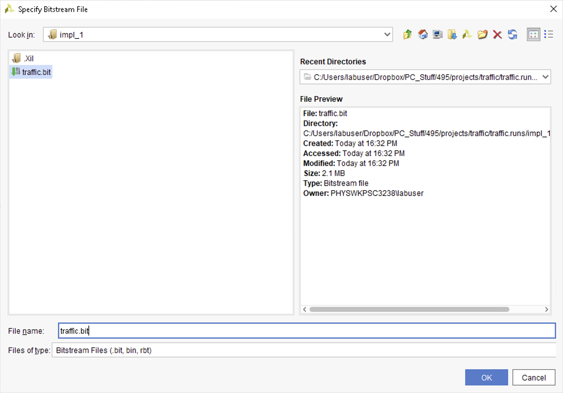
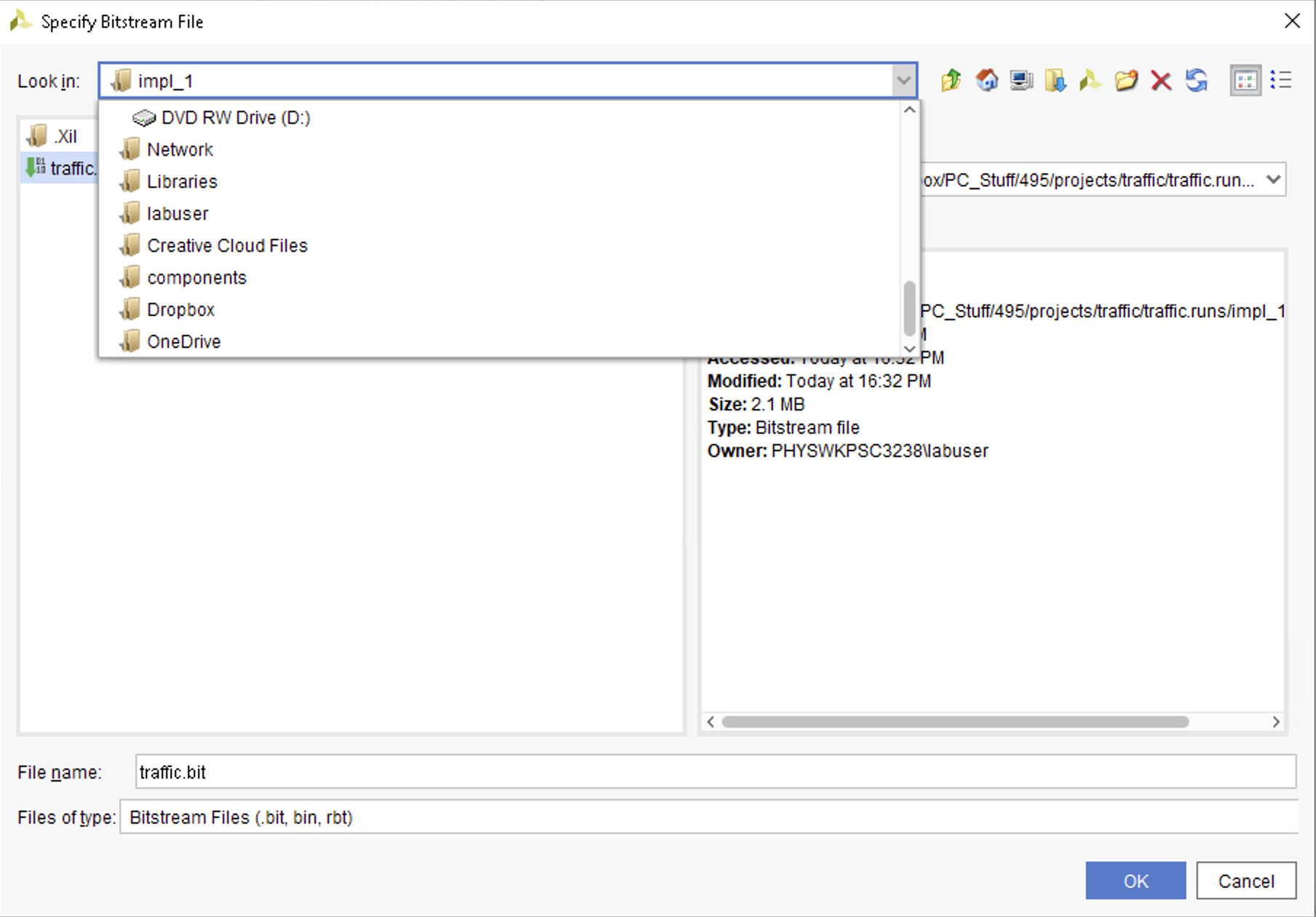
Don't trust that it put you in the right directory! Click on the
downward carot in the "Look in:" line:
and browse to the directory that you have everything in for this project.
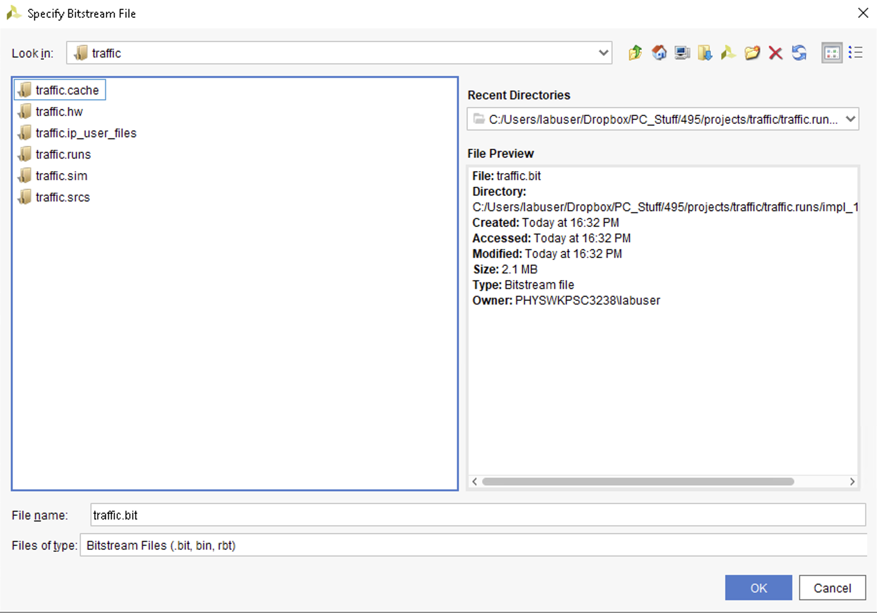
For my project, it will show you this:
Source files are in "traffic.srcs", and bitstream files are in
"traffic_runs/impl_1". You should see a file called "traffic.bit".
Select that file (double click) and it will show up in the
"Bitstream file:" line. Then click "Program", and it should go fast.
Now, if you turn enable on by pushing the bottom toggle switch up,
then you should see the lights changing. If you see all 3 LEDs on,
then that probably means you have very short times for the counters
(which we did just to see the simulation work), and they are blinking
so fast that it looks like they are always on. So you will have to go
back to your code and check, and then run through everything again.
That means make sure in your Verilog code, the done conditions look
something like this:
As discussed above, you can send the program into the onboard flash ram,
so that the board will power up and load the program automatically.
To accomplish this, first move the jumper on J1 to the QSPI position
(see Basys3 photo above, J1 is item 10,
the jumper should connect the first
2 pins closest to the edge).
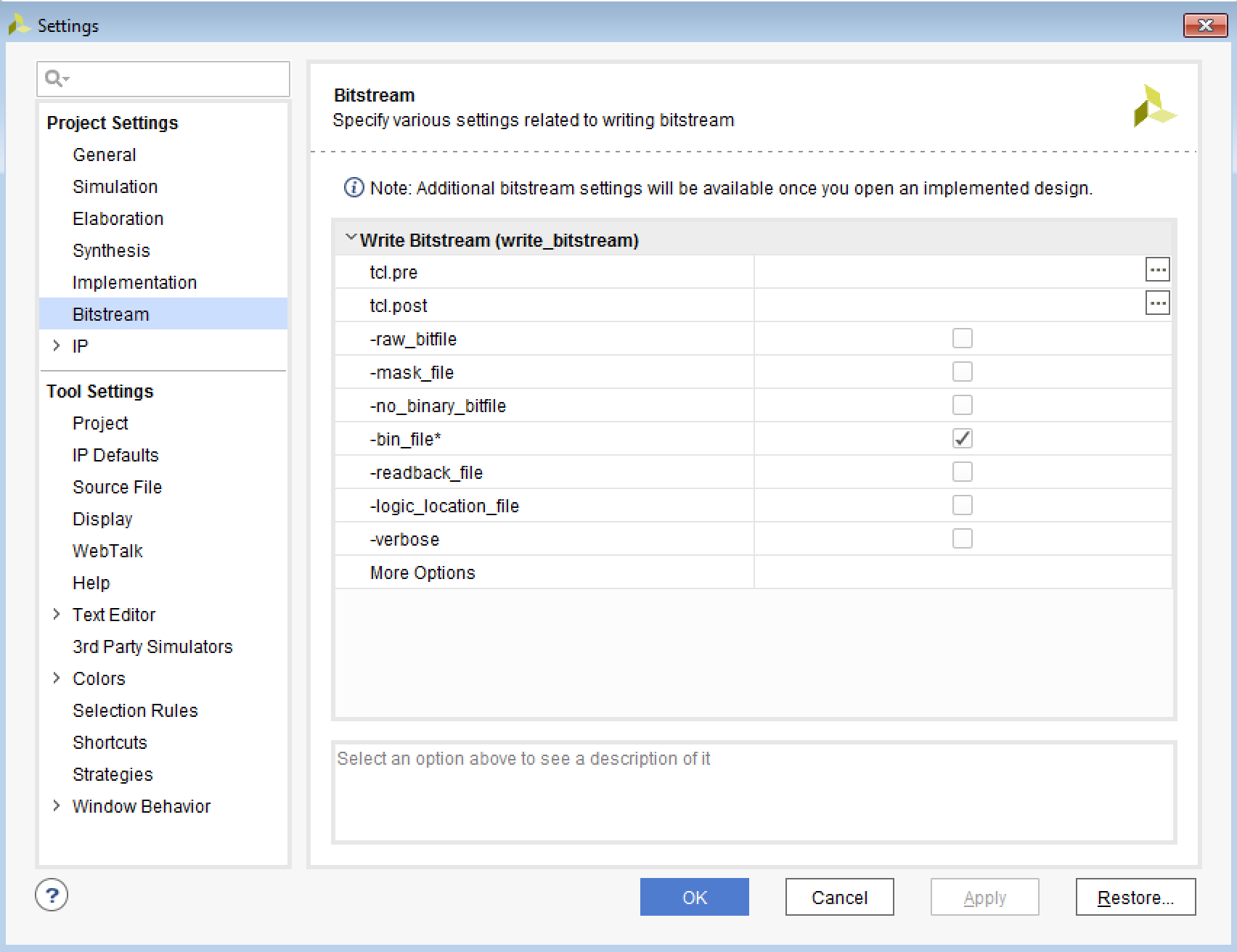
The file that is sent to the flash over the USB cable is a .bin file,
and has to be created when you "Generate Bitstream". To ensure this,
right click on "Generate Bitstream" and select "Bitstream Settings".
That will produce a popup window that looks like this:
Click on "Bitstream" in the left panel "Project Settings", select
"-bin_file*", and hit OK. Then generate the bitstream. It should
make the *.bin file, in the same place (*_runs/impl_1/*.bin)
as the *.bit file.
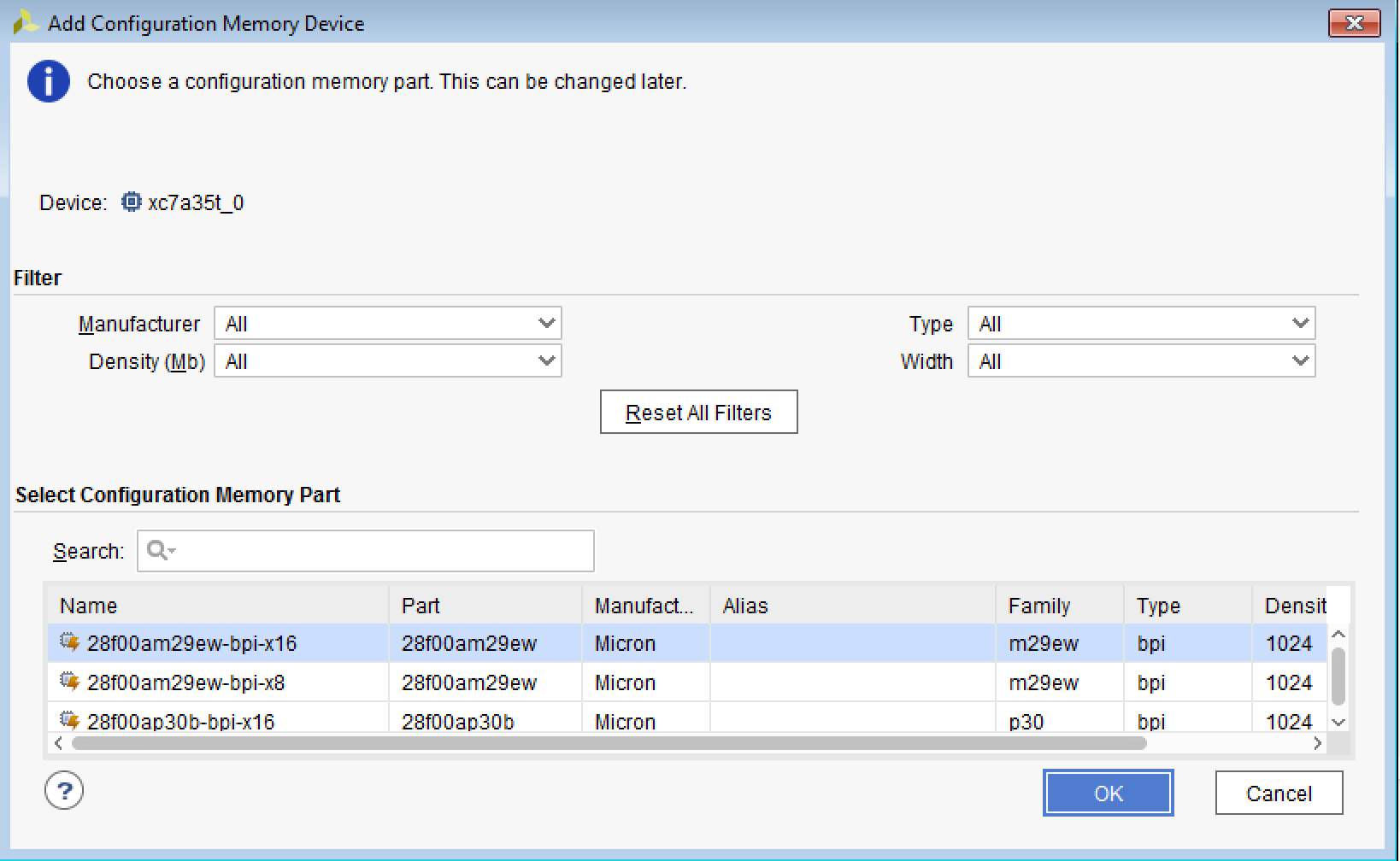
Now you have to tell Vivado about the flash memory, so it can download
to it. The easiest way to do this is to click on
"Add Configuration Memory Device" in the hardware manager and select
the device "xc7a35t_0"
This will bring up a new window called "Add Configuration Memory Device":
In the "Search:" text area, type in the flash device name, which is
found on page 6 of the basys3_rm.pdf file: S25FL032. That should bring
up the correct name in the list below the search field. Click on that
name and hit OK. If all is well, you should see something like this
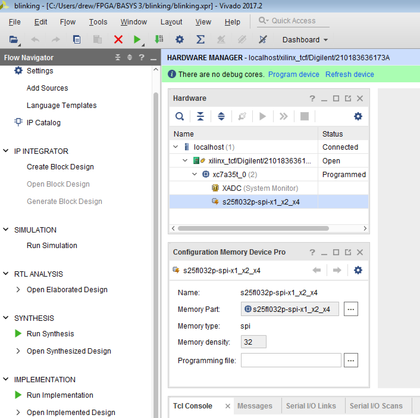
in the "Hardware" panel:
Then all you have to do is right click on the memory part
(s25fl032p-spi-x1_x2_x4) and select "Program Configuration Memory Device".
It will pop up yet another window asking for the .bin file. Navigate
to it in the "Configuration file:" text window (again, it's in the
directory *.runs/impl_1 where * is the project name), select the .bin
file, and hit OK, and hit OK again in the "Program Configuration Memory Device"
window. It will then show a progress window where it first erases, and then
programs the flash. It will take probably 30 seconds or so, and if all
goes well will show a window that says "Flash programming completed successfully".
Hit ok.
The last thing you need to do now is to actually load the program from
flash into the FPGA by pushing the "PROG" button (item 9 in
the Basys3 photo above). It takes about 5
seconds.
Verilog Traffic Light FSM
    module traffic(
        input clock, enable, reset,
        output reg red, green, yellow
    );
Note that the outputs are all registers, since they are being driven by the
FPGA.
    //
    //  now for the counters used for the timers.   we will use
    //  10sec for red and green and 2sec for yellow.
    //  the input clock is 10ns.
    //  so to get to 10sec, we will need 10^9 ticks of the clock.
    //  which menas around a 30bit counter.
    //
    //  let's use a 32-bit counter so that we can go to 30sec if we
    //  want to.
    //
    reg [31:0] rTimer, gTimer, yTimer;
To implement the done lines for the 3 colors, all we need to do is count
a certain number of ticks, which we can do with code like this:
    //
    //  the done lines will count to 100,000,000 for red and green
    //  and 20,000,000 for yellow
    //
    wire yDone = (yTimer == 'd20000000);
    wire gDone = (gTimer == 'd100000000);
    wire rDone = (rTimer == 'd100000000);
The 3 timers will only start counting when the corresponding light is on, so
we can implement the counters with code like this:
    //
    //  next implement the counters
    //
    always @ (posedge clock) begin
        if (reset) begin
            //
            //  you need a reset to define things for the simulation, but the FPGA
            //  will just set these to 0 to start
            //
            rTimer <= 0;
            gTimer <= 0;
            yTimer <= 0;
        end
        else begin
            //
            if (red) rTimer <= rTimer + 1;
            else rTimer <= 0;
            if (green) gTimer <= gTimer + 1;
            else gTimer <= 0;
            if (yellow) yTimer <= yTimer + 1;
            else yTimer <= 0;
        end
    end
    //
    //  next implement the counters
    //
    always @ (posedge clock or posedge reset) begin
    .
    .
    .
Either way, both are fine but here, 10ns is pretty fast compared to the time the
lights are on so the reset will happen pretty much instantaneously anyway.
    //
    //  implement the state machine
    //
    //  we need 4 states:  a WAIT state to wait for enable,
    //  and 3 states for the RED, GREEN, and YELLOW.
    //  so a parameter that has 2 bits can implement 4 values:
    //
    parameter [1:0] WAIT=0, RED=1, GREEN=2, YELLOW=3;
    //
    //  and a state variable that can hold 4 values
    //
    reg [1:0] state;
For the FSM, we can use a synchronous reset. But we have to take care about
the enable. For instance, what happens when in the middle of a cycle, the
enables goes away? If the FSM is in the RED state, then let's tell it to
go back to the WAIT state. If it's in the GREEN state, let's not jump
right back into red, but let it finish and then go to YELLOW and then go
back to RED, so that if enable is still down when it is back into RED, it
will stay there (or go to the WAIT state). The code might look like this:
    //
    //  and the FSM:
    //  for the WAIT state, let's be safe and turn the red light on!
    //  we will use the case statement to implement the FSM
    //
    always @ (posedge clock) begin
        if (reset) begin
            state <= WAIT;
            red <= 1;
            green <= 0;
            yellow <= 0;
        end
        else begin
            case (state)
                WAIT: begin
                    red <= 1;
                    green <= 0;
                    yellow <= 0;
                    if (enable) state <= RED;
                    else state <= WAIT;
                end
                RED: begin
                    //
                    //  note that in the RED state, if enable goes
                    //  away, then we want to go into the WAIT state
                    //
                    red <= 1;
                    green <= 0;
                    yellow <= 0;
                    if (enable) begin
                        if (rDone) state <= GREEN;
                        else state <= RED;
                    end
                    else state <= WAIT;
                end
                GREEN: begin
                    //
                    //  in GREEN, if enable goes away, then we don't
                    //  want to jump right back into RED, it could cause
                    //  collisions!  so just finish and go to YELLOW as usual
                    //
                    red <= 0;
                    green <= 1;
                    yellow <= 0;
                    if (gDone) state <= YELLOW;
                    else state <= GREEN;
                end
                YELLOW: begin
                    red <= 0;
                    green <= 0;
                    yellow <= 1;
                    if (yDone) state <= RED;
                    else state <= YELLOW;
                end
            endcase
        end
    end
Note that in each state, we specify the value for the red, green, and yellow lights
just to be sure that they are all set for all states explicitly.
Verilog Testbench
module TRAFFIC_tb;

    reg clock_in;
    reg reset_in;
    reg enable_in;
    wire red_out, green_out, yellow_out;
    wire illegal_out;
    traffic my_traffic(
        .clock(clock_in),
        .reset(reset_in),
        .enable(enable_in),
        .red(red_out),
        .green(green_out),
        .yellow(yellow_out)
        );

endmodule
Note: TRAFFIC_tb is driving inputs into traffic, and looking at outputs,
but has no input/outputs of its own. So you just need a semicolon
after the "module TRAFFIC_TB" declaration.
    parameter PERIOD = 10.0;
    always begin
        clock_in = 1'b0;
        #(PERIOD/2) clock_in = 1'b1;
        #(PERIOD/2);
    end
Notes on the above:
    initial begin
        reset_in = 0;
        enable_in = 0;
    end
The Verilog "initial" statement
does just that, initializes things. Since we
set it to 0 and don't change it, it will stay at 0. So to make it change, we
do this:
    initial begin
        reset_in = 0;
        enable_in = 0;
        #50 reset_in = 1;
        #20 reset_in = 0;
        #100 enable_in = 1;
    end
So what we are doing is the following:
Running the simulation
//    wire yDone = (yTimer == 'd20000000);
//    wire gDone = (gTimer == 'd100000000);
//    wire rDone = (rTimer == 'd100000000);
    wire yDone = (yTimer == 'd200);
    wire gDone = (gTimer == 'd1000);
    wire rDone = (rTimer == 'd1000);
Connecting FPGA pins to the project
The Basys 3 board includes a single 100 MHz oscillator connected to pin W5
That means that the clock chip output goes into the FPGA on pin W5. Now
all we need to do is learn how to connect pin W5 to the "clock" line on
the input to traffic.v.
Verilog FPGA pin
clock W5
enable V17
reset U18
red U16
green E19
yellow U19
# clock
set_property PACKAGE_PIN W5 [get_ports clock]
set_property IOSTANDARD LVCMOS33 [get_ports clock]
The hash mark # means a comment. The "set_property" has 2 variations
we will use: PACKAGE_PIN and IOSTANDARD. PACKAGE_PIN means what pin on
the FPGA, here it will be W5, which is the clock pin as described above.
Then inside the [] you put the name of the Verilog "port" (specified in
the Verilog input), which is "clock". IOSTANDARD allows you to specify
whether you want to use "single ended" (a single voltage) or differential.
We will use LVCMOS33, which means "low voltage" CMOS, 3.3 volts from 0 to 1.
That is, 0 volts means a logic 0 and 3.3 volts means a logic 1. This is
pretty much a standard for FPGAs, although there are lots others.
# clock
set_property PACKAGE_PIN W5 [get_ports clock]
set_property IOSTANDARD LVCMOS33 [get_ports clock]
# reset
set_property PACKAGE_PIN U18 [get_ports reset]
set_property IOSTANDARD LVCMOS33 [get_ports reset]
# enable
set_property PACKAGE_PIN V17 [get_ports enable]
set_property IOSTANDARD LVCMOS33 [get_ports enable]
# red
set_property PACKAGE_PIN U16 [get_ports red]
set_property IOSTANDARD LVCMOS33 [get_ports red]
# green
set_property PACKAGE_PIN E19 [get_ports green]
set_property IOSTANDARD LVCMOS33 [get_ports green]
# yellow
set_property PACKAGE_PIN U19 [get_ports yellow]
set_property IOSTANDARD LVCMOS33 [get_ports yellow]
Synthesis
The synthesis stage is where Vivado
takes the logic from the Verilog program and checks for syntax, errors,
etc, and any constraints you might have (that's another story, we won't
use constraints). The synthesizer will take your Verilog "high level"
code and turns it into a gate level representation, which is also called
a "netlist", which tells the system what resources are needed and
how they are connected.
Implementation
Bitstream Generation
Setting up the BASYS3 board
Downloading (Hardware Manager)
For now, let's do the fast one and just program it directly (volatile).
So in the "Program Device" popup, it will ask you for the "Bistream File".
Click on the 3 dots to browse to the bitstream file, which will be in
the same directory as all of the sources for your project. So you should
see something like this:
    wire yDone = (yTimer ==  'd200000000);
    wire gDone = (gTimer == 'd1000000000);
    wire rDone = (rTimer == 'd1000000000);
Programming Flash Ram
All rights reserved. No part of this publication may be reproduced, distributed, or transmitted in any
form or by any means, including photocopying, recording, or other electronic or mechanical methods, without
prior written permission, except in the case of brief quotations embodied in critical
reviews and certain other noncommercial uses permitted by copyright law.
Unless indicated otherwise, any lecture handouts, exams, homework and exam solutions,
and the lectures themselves (including audio and video recordings) are copyrighted by
me and may not be distributed or reproduced for anything other than your personal use
without my written permission.
Last updated October, 2023 Drew Baden