Carbon Nanotube Electronics
Introduction to
Carbon Nanotubes
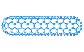
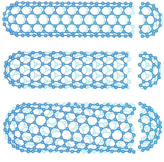
Carbon nanotubes are wires of pure carbon with nanometer
diameters and lengths of many microns. A single-walled carbon
nanotube (SWNT) may be thought of as a single atomic layer thick sheet of
graphite (called graphene) rolled into a seamless cylinder. Multi-walled
carbon nanotubes (MWNT) consist of several concentric nanotube shells.
Understanding the electronic properties of the graphene sheet
helps to understand the electronic properties of carbon nanotubes.
Graphene is a zero-gap semiconductor; for most directions in the graphene sheet,
there is a bandgap, and electrons are not free to flow along those directions
unless they are given extra energy. However, in certain special directions
graphene is metallic, and electrons flow easily along those directions.
This property is not obvious in bulk graphite, since there is always a
conducting metallic path which can connect any two points, and hence graphite
conducts electricity.
However, when graphene is rolled up to make the nanotube, a
special direction is selected, the direction along the axis of the nanotube.
Sometimes this is a metallic direction, and sometimes it is semiconducting, so
some nanotubes are metals, and others are semiconductors. Since both metals and semiconductors can be
made from the same all-carbon system, nanotubes are ideal candidates for
molecular electronics technologies.
In addition to their interesting
electronic structure, nanotubes have a number of other useful properties.
Nanotubes are incredibly stiff and tough mechanically -
the world's strongest fibers. Nanotubes conduct heat as well as diamond at
room temperature. Nanotubes are very sharp, and thus can be used as probe
tips for scanning-probe microscopes, and field-emission electron sources for
lamps and displays.
See also the following review articles:
"Single-Walled Carbon Nanotube Electronics,"
Paul L. McEuen, Michael S. Fuhrer, Hongkun Park, IEEE Transactions on
Nanotechnology, 1, 78 (2002).
(download PDF Format)
"Single-wall
Carbon Nanotubes," Paul L. McEuen, Physics World, June 2000
(download PDF Format)
"Single-Walled Carbon Nanotube
Electronics," M. S. Fuhrer, in Advanced Semiconductor and Organic Nano-Techniques,
H. Morkoc, Ed. (Academic Press, New York, 2003).
(download introduction in PDF format)
(visit
book web page)
Device
Fabrication
Find 'em and wire 'em
In the Fuhrer lab we have developed techniques for synthesizing
carbon nanotubes directly on silicon substrates, locating individual nanotubes,
and electrically contacting nanotubes with metallic electrodes. The
general idea is to "find 'em and wire 'em", as opposed to attempting to
self-assemble nanotubes in place, or deposit nanotubes or wires at random and
hope to contact some nanotubes. The great advantage of the find 'em and
wire 'em technique is that we can make customized devices. Some examples
are below.
|
 |
 |
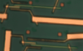
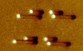
| Atomic force microscope
(AFM) image of crossed nanotubes (green) contacted by Au electrodes
(yellow) using the "find 'em and wire 'em" technique. In this work,
performed at UC Berkeley, the nanotubes were deposited onto the chip from
solution, and located using the AFM. |
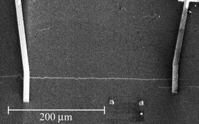
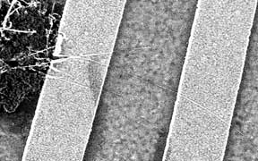
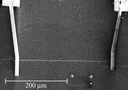
Scanning electron microscope
(SEM) image of a long nanotube transistor fabricated at Maryland using the
"find 'em and wire 'em" technique. The nanotube is the thin horizontal white line
connecting the two gold leads (thicker vertical lines). Here the
nanotubes were grown by chemical vapor deposition directly on the
substrate, and located using the SEM. |
The disadvantages of the find 'em and wire 'em scheme are that
we are able to make only a limited number of devices, and the technique is not
"scalable" - that is, making twice as many devices takes twice as much time.
If nanotubes are to find electronic applications in industry, scalable
fabrication techniques will be needed. However, our current techniques
allow us to jump ahead and explore single nanotube devices, to see if they have
the useful properties that would warrant developing techniques to mass produce
devices.
CVD growth of nanotubes
Largely following research by the
Dai Group
at Stanford and the Lieber Group at
Harvard, we are using chemical vapor deposition (CVD) to prepare our carbon
nanotubes. The basic ingredients needed for CVD growth of nanotubes are a
small catalyst particle (typically iron or iron/molybdenum) and a hot
environment of carbon-containing gas (we use CH4 and C2H4).
The metal particle catalyzes the decomposition of the carbon-containing gases,
and the carbon dissolves in the catalyst particle. Once the catalyst
particle is supersaturated with carbon, it extrudes out the excess carbon in the
form of a tube. One catalyst particle of a few nanometers in diameter can
produce a nanotube millimeters in length, about 1 million times the size of the
particle.
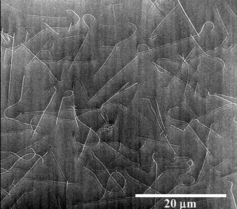 |
| Nanotubes grown by the CVD process on a silicon
dioxide covered silicon chip. The thin white lines are the nanotubes.
The nanotubes here form a continuous conducting network, and thus are too
dense to use for device fabrication. |
Typically we use silicon chips (pieces of flat silicon wafer
from the semiconductor industry) as our substrate material, with a layer of
silicon dioxide (glass) grown on top of the silicon as an insulator. The
catalyst con be obtained in several ways; the easiest is to dip the silicon chip
into a solution of ferric nitrate in isopropanol, and then dip the chip into
hexane to cause the ferric nitrate to come out of solution. This deposits
nanocrystals of ferric nitrate on the chip, which can be reduced to iron with
hydrogen in the growth furnace.
Locating the nanotubes
Once the nanotubes are grown on the substrates, we need to
locate them. To do this, we first deposit a pattern of alignment marks on
the substrate, using a conventional lithography technique (actually we use
electron-beam lithography, but optical lithography would work as well).
Our original method for locating nanotubes was to use the atomic force
microscope (AFM). The AFM uses a tiny needle on the end of a
diving-board-like cantilever to tap on a surface as it scans over that surface.
It sense the amplitude of the tapping and use that to follow the height
variations in the surface, making a topographical map of the area. The AFM
is very sensitive, so it is able to image the nanometer-diameter nanotubes lying
on the flat substrate. However, AFM is very time consuming, taking 5
minutes or so to image a 10 x 10 micron square image.
Recently we have developed a technique to image nanotubes using
the scanning electron microscope (SEM). This imaging technique relies on
the fact that the nanotubes are conducting, and the substrate on which they are
lying is insulating. The SEM images by scanning a high-energy beam of
electrons over the sample. Secondary electrons generated by the energetic
beam are collected and amplified to produce the image signal. When the SEM
beam hits an insulator, some electrons stick in the insulator and it becomes
negatively charged. When the beam scans over the nanotube, the electrons
are free to spread out along the nanotube, and thus the area around the nanotube
is less negatively charged. The less negatively charged area allows more
electrons from the substrate to escape and be detected, producing a signal when
the beam scans across the nanotube. Examples of SEM and AFM images of
nanotubes are seen below.
|
 |
|
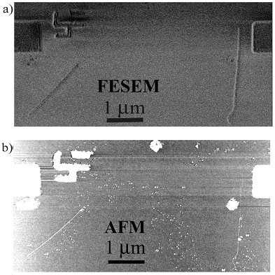
Comparison
of field-emission scanning electron microscope (FESEM) and atomic force
microscope (AFM) images of nanotubes (two narrow lines) and Cr/Au
alignment markers (squares and geometric shapes). The FESEM (a) images the
conducting alignment marks and nanotubes, but is insensitive to the
surface contamination visible in the AFM image (b). The FESEM image was
acquired approximately 100 times faster than the AFM scan.
|
Once the nanotubes are located, they may be contacted
electrically using electron-beam lithogrpahy (EBL). A thin layer of resist
(a polymer) is spun onto the chip, and the SEM is used again, but this time the
energetic electron beam is used to write a pattern in the resist where we want
the electrodes to be. The resist which has been exposed to the beam is
then washed away in a solvent, and metal (such as gold) is evaporated into the
holes in the resist, forming wires which contact the nanotubes. The excess
metal which is on top of the resist is lifted off of the chip using a second
solvent which dissolves the remaining resist. The electrodes for both the
crossed nanotube device and the long nanotube device shown above were fabricated
using EBL.
Electrical measurements
The wires on the chip are much bigger than the nanotube,
but still fairly small - typically the largest parts of the wires on the chip
are one or two tenths of a millimeter across. We make contact to the wires
on the chip under a microscope, either by using a wire bonder which can attach
larger wires to the chip to connect it to a rigid chip holder, or by using a
probe station, which has sharp needles that can be used to temporarily make
contact to the wires on the chip.
Once electrical contacts are made to the nanotubes, we can
test their electrical properties. The simplest nanotube device has just
two electrode, one at each end of the nanotube. There is actually a third
electrode, called the gate, which is the silicon substrate underneath the
nanotube. This electrode is not in electrical contact with the nanotube,
since it is separated from the nanotube by an insulator (typically silicon
dioxide). However, the capacitor formed by the nanotube and the gate can
be charged by applying a voltage between nanotube and gate. This way we
can change the amount of charge on the nanotube.
When we change the gate voltage (changing the amount of
charge on the nanotube) and measure the conductance between the two contacts on
the nanotube (conductance is the inverse of resistance) we see one of two types
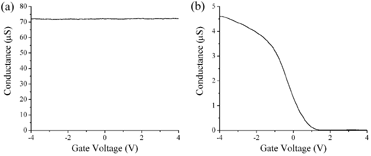
of behavior. Either the conductance stays constant as we change the gate
voltage, or it drops dramatically as we make the gate voltage more positive (see
below). We identify the first type of behavior with the metallic nanotubes
- changing the charge on a metal does not change its conductance. The
second type of behavior we associate with the semiconducting nanotubes - unless
they are "doped", semiconductors don't have any charges which can carry current.
The gate voltage allows us to add charge to the nanotube and make it conduct.
Negative gate voltage adds "holes" (positive charges corresponding to the
absence of an electron) to the nanotube, and it conducts better. Around
zero gate voltage there are no holes, and the nanotube stops conducting.
(The nanotube should conduct again at a positive enough voltage which
would add negatively charged electrons to the nanotube, but it doesn't for
reasons related to a barrier at the metal-nanotube interface.)
|
 |
|
Conductance
as a function of gate voltage for (a) a metallic nanotube, and (b) a
semiconducting nanotube.
|
See also the following publications for more
information:
"Rapid Imaging of Nanotubes on Insulating Substrates" T. Brintlinger, Yung-Fu
Chen, T. Dürkop, Enrique Cobas, M. S. Fuhrer, John D. Barry, and John Melngailis,
Applied Physics Letters 81, 2454 (2002).
(download PDF format)
"Single-Walled Carbon Nanotube Electronics,"
Paul L. McEuen, Michael S. Fuhrer, Hongkun Park, IEEE Transactions on
Nanotechnology, 1, 78 (2002).
(download PDF Format)
"Single-wall
Carbon Nanotubes," Paul L. McEuen, Physics World, June 2000
(download PDF Format)
"Single-Walled Carbon Nanotube
Electronics," M. S. Fuhrer, in Advanced Semiconductor and Organic Nano-Techniques,
H. Morkoc, Ed. (Academic Press, New York, 2003).
(download introduction in PDF format)
(visit
book web page)
Conductance and Mobility
Recently, much of our research has focused on semiconducting
nanotubes, because of their utility for devices. Since the conductance of
the semiconducting nanotube can be changed by the voltage on a third electrode
(the gate), the nanotube acts like a switch. This type of switch is called
a field-effect transistor (FET), and forms the basis of most computer chips used
today. We are very interested in determining how well nanotubes perform as
field-effect transistors, in order to gauge their prospects for future
electronics applications.
The first question one might ask is: How well do semiconducting
nanotubes conduct? The figure below shows the conductance of a very long
nanotube (about 1/3 of a millimeter long) as a function of gate voltage.
The highest conductance observed is 1.6 micro-Siemens, which corresponds to a
resistance of around 600 kilo-Ohms. How does this compare to other
materials? In order to compare, we need to consider the conductivity,
conductance x length/area. This takes into account the fact that we expect
a long, thin wire to have lower conductance than a short, fat wire. The
conductivity of the nanotube is around 2.6 micro-Ohm-centimeters. This is
comparable to good metals like copper (1.6 micro-Ohm-centimeters), which is very
surprising. This means that this nanotube switch can be tuned from
insulating, to conducting as well as copper, simply by changing the gate
voltage!
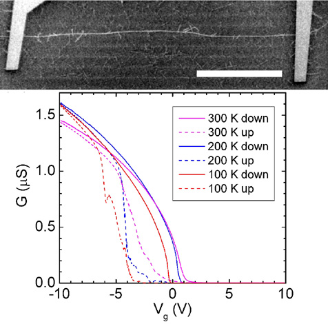 |
| The top panel shows an SEM image of a long
semiconducting carbon nanotube spanning between two gold electrodes (scale
bar is 100 micrometers). The bottom graph shows the conductance of
this nanotube as a function of the voltage applied to the back gate
(silicon substrate) at temperatures of 300, 200, and 100 Kelvins. |
The above analysis also hints that conductivity isn't the best number to use
when comparing one semiconductor to another, since the conductivity
changes with charge density (in this case with gate voltage). It's fine
for metals, like copper, where the charge density is very high and doesn't
change much. The number that's used to indicate how well one semiconductor
conducts compared to another is mobility. Mobility is the
conductance divided by the density of charge carriers, so it can be used to
compare the conductance of semiconductor samples with different amounts of
charge to carry the current.
We know the charge density in our nanotube devices, because we know the
capacitance C between the nanotube and the gate electrode that is
producing the charge. The charge Q is proportional to the capacitance and
to the amount of gate voltage V we have applied: Q = CV.
So we know everything we need to find the mobility. The mobility of one of
our long nanotube transistors is shown below.
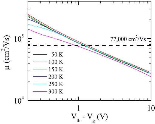 |
| Mobility as a function of gate voltage for a
semiconducting carbon nanotube. At low gate voltage (low charge
carrier density) the mobility exceeds that of InSb (77,000 cm2/Vs),
the previous highest-known mobility at room temperature. |
The mobility is higher than 100,000 cm2/Vs at room temperature,
higher than any other known semiconductor. (The previous record, for InSb,
was 77,000 cm2/Vs, set in 1955.) The mobility is a function of
the gate voltage, and is higher when the gate voltage is low, i.e. when there
are fewer charges in the devices. We don't know why this is yet, but we
are studying this. The mobility is also rather independent of temperature,
suggesting that the thermal vibrations of the lattice, called phonons, don't
play much of a role in scattering the electrons.
Why is the mobility so high? Part of the reason is that graphite itself
is a good conductor of electricity. The mobility of charges in graphite is
around 20,000 cm2/Vs at room temperature. Graphite also has
other excellent properties - it's strong, lightweight, and an excellent
conductor of heat. But graphite isn't a semiconductor - it doesn't have a
bandgap - so it can't be used to make semiconductor devices like transistors.
The nanotube can be thought of as a way to engineer a bandgap in graphite so we
can use it for semiconductor devices (see Introduction to
Carbon Nanotubes above). The mobility in nanotubes turns out to be
even higher than in graphite. Part of the reason for this may lie in the
one-dimensional nature of the nanotube - it's harder to scatter electrons in
one-dimension, because they can only go forward or backward, not to the sides.
See also the following publications:
"Extraordinary Mobility in Semiconducting Carbon Nanotubes," T. Dürkop, S. A.
Getty, Enrique Cobas, and M. S. Fuhrer, Nano Letters ASAP (Web Release
Date: 03-Dec-2003).
(download PDF Format)
"High-Mobility Semiconducting Nanotubes," T. Dürkop, E. Cobas, and M. S. Fuhrer in Molecular
Nanostructures, pp. 524-7, H. Kuzmany, J. Fink, M. Mehring, and S. Roth,
Editors (AIP Conference Proceedings, New York, 2003).
(download PDF Format)
"Nanotubes are High Mobility Semiconductors," T. Dürkop,
T. Brintlinger, and M. S. Fuhrer in Structural and Electronic Properties of Molecular
Nanostructures, pp. 242-6, H. Kuzmany, J. Fink, M. Mehring, and S. Roth,
Editors (AIP Conference Proceedings, New York, 2002).
(download PDF Format)
"Ballistic Transport in Semiconducting Carbon Nanotubes" M. S. Fuhrer, M.
Forero, A. Zettl, P. L. McEuen, in Electronic Properties of Molecular
Nanostructures, pp. 401-4, H. Kuzmany, J. Fink, M. Mehring, and S. Roth,
Editors (AIP Conference Proceedings, New York, 2001).
(link to paper on AIP website)
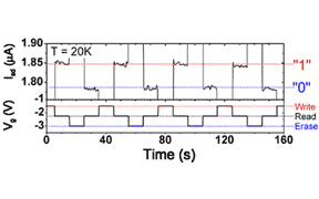
Nanotube
Single-Electron Memory
See also the following publications:
"Single-Electron Detection and Memory Using a Single Carbon Nanotube Defect",
B.M. Kim, Y.F. Chen, and M.S. Fuhrer, in Fullerenes Volume 12: The Exciting
World of Nanocages and Nanotubes, pp. 541-548, P. Kamat, D. Guldi, and K.
Kadish, Editors (ECS Conference Proceedings, 2002).
(download PDF Format)
"High-Mobility Nanotube Transistor Memory" M. S. Fuhrer, B. M. Kim, T. Dürkop, and T.
Brintlinger, Nano Letters 2, 755 (2002).
(download PDF format)
Spin Transport
in Nanotubes
Coming soon...
High Performance
Nanotube FETs on SrTiO3
Coming soon...