There are many ways that we can use "digital" to become more like "analog". One of the more useful is called "pulse width modulation".
To start, let's start a new project (maybe call it PWM), input the clock and one of the 16 switches, and output the 16 LEDs, and investigate what happens when we drive the leds with a clock-like signal that is slower than the 100MHz "clk" signal. We have 16 LEDs, and we probably want to have one of them either on or off for comparison purposes (we can use the switch for that), one of them to be driven by the 10ns clock, and ther other 14 to be driven by a counter so that each bit of the counter will be toggling at a different rate (each bit will be half the rate of the bit before it). So to do this we make a 14-bit counter, like this:
`timescale 1ns / 1ps

module top(
    input clk,
    input sw0,
    output [15:0] led
    );

    //
    // make a 14 bit counter to turn on and off all 16 LEDs with different pulse widths
    //
    reg [13:0] counter;
    always @ (posedge clk) counter <= counter + 1;
    //
    assign led[15:0] = {counter[13:0],clk,sw0};
endmodule
The statement "assign led[15:0] = {counter[13:0],clk,sw0};" is called a
Verilog "concatenation", and is actually 16 statements in one. The
assignment says that we want to connect led[15] to counter[13], then
led[14] to counter[12], and so on down to led[1] connected to clk and
led[0] connected to sw0.
We have turned on the 1st led (led[0] using the lowest switch (sw0, the one closest to the right), so that that LED is driven by a signal that is always up (100% duty factor). The next led (led[1]) is driven by the 10ns clock, the next one (led[2]) by the lowest bit of the counter, which will change every 20ns (20ns clock), and so on all the way up to the last bit. Since we know that counter[0] is equivalent to a 20ns clock, then we can calculate the period of each counter[n]: T_n=10ns× 2n+1. The highest bit, counter[13], will have a period of T13 = 10ns × 16384 = 163.84μs. The following picture shows the result.
By using a higher counter bit, we get a brighter signal even though the duty factor is still 50%. This is because the 10ns clock is only on (3.3volts) for 5 ns, which is not enough time for the LED to fully turn on. However, the highest led will be on for half the period of the driving clock, which will be 81.92μs, long enough to become almost as bright as the bottom led which is always on.
Changing the Duty Factor
Now let's investigate how we can change the duty factor, and see how this effects things. The easiest way to do this is to generate our own pulse, and control how long it stays on and how long it stays off. We will define two counters counters called count_on and count_off, which counts 10ns ticks. The former will control how long the pulse is on, and the latter how long it is off. The targets will be stored in two other registers called on and off (both are of course busses), and we can make them the same length although they can be shorter. We will use the counters to count 10ns ticks to control when the output goes on, and when it goes off, thus sculpting our own square wave pulse. The pulse will be in the register OUT, which we can use to drive an led or even bring out onto one of the output pins.
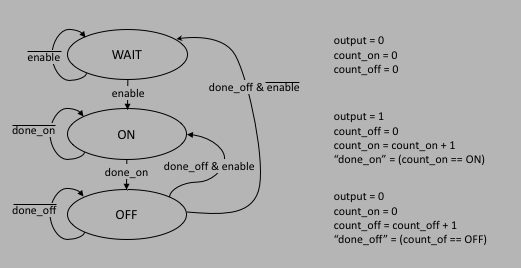
To control it, we will make a state machine that waits for some kind of enable (perhaps using the bottom switch on/off) so that we can make sure all counters and outputs are under control. When the state machine is enabled, it turns on the output (OUT <= 1), and starts counting. When the counter reaches the value specified by on, we turn the output off (OUT <= 0) and start another counter. When that counter is equal to the value stored in off, we go back to the ON state and repeat (unless the enable goes away). The size of the register busses count_on and count_off (and on and off) determine the width of the pulse, given by width = on + off.
The state machine diagram will look something like the following:
The code will look something like this:
module top(
    input clk,
    input [15:0] sw,
    input btnU,             // reset
    output [15:0] led
    );

    //
    // turn the FSM on using sw[15];
    //
    wire enable = sw[15];
    //
    // let's say we want 1024 times the clock period for period of the output signal
    //
    // for the ON and OFF registers, we will use the bottom 10 switches.
    // so full scale 100% duty factor will be ON='h3FF and OFF = 0, so the calculation
    // we need is:
    //
    wire [9:0] on, off;
    assign on = sw[9:0];
    assign off = 'h3FF - on;
    //
    // now make the counters and the output and the FSM
    //
    reg [9:0] count_on, count_off;
    reg OUT;
    localparam [1:0] WAIT=0, ON=1, OFF=2;
    reg [1:0] state;
    always @ (posedge clk)
        if (btnU) begin
            state <= WAIT;
            OUT <= 0;
        end
        else case (state)
            WAIT: begin
                OUT <= 0;
                count_on <= 0;
                count_off <= 0;
                if (enable) state <= ON;
                else state <= WAIT;
            end
            ON: begin
                OUT <= 1;
                count_off <= 0;
                count_on <= count_on + 1;
                if (count_on == on) state <= OFF;
                else state <= ON;
            end
            OFF: begin
                OUT <= 0;
                count_on <= 0;
                count_off <= count_off + 1;
                if (count_off == off) begin
                    if (enable) state <= ON;
                    else state <= WAIT;
                    end
                else state <= OFF;
            end
            default: begin
                OUT <= 0;
                count_on <= 0;
                count_off <= 0;
                state <= WAIT;
            end
        endcase
    //
    // now drive the output onto led[15], and have the lower 10 led's follow the switches
    //
    assign led = {OUT,5'b00000,on[9:0]};
endmodule
Switch sw[15] turns the thing on (wire enable = sw[15]), and we have made the
register busses be 10 bits wide, which means our pulse will be 1024× 10ns = 10.24μs
wide. Note that in the code, we set the on and off registers so that the sum adds
up to 10'h3FF = 1023 decimal. The value for on comes from the bottom 10 switches, and
off is set to 10'h3FF-off. For a 50% duty factor, you would set on = 512 decimal
(turn on all 9 bottom switches).
If you start with all the other switches off, you will see no pulse (on=0!). Then start turning the switches on one at a time, and you can see the pulse on led[15] brighten as you increase the on time and decrease the off time. Note: by changing the switches, you change the duty cycle, but the period of the pulse stays the same (10.24μs).
Modulating the Duty Factor
The next step is where it gets interesting: we want to change the on register so that it's not determined by the switches, but instead is itself changing over time. This is the "modulation" in "pulse width modulation".
All we need to add now is the ability to dynamically change the value of the on and off registers in the above state machine. The most straightforward way to do this would be to add a new state after the "OFF" state, and put all the logic there that will be necessary in order to decide when to change the pulse width, and by how much. We will call this new state "CHANGE". The state machine diagram is below:
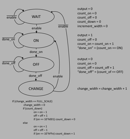
On the right, we see the registers that change as a matter of course. Below the "CHANGE" state, we see the logic that is implemented. Note that one has to be extremely careful here - FPGAs are not computers, and you have to remember to keep in mind that all things happen at the posedge of the clock, simultaneously.
The logic consists of the following:
The full code for top.v is shown below:
`timescale 1ns / 1ps
module top(
    input clk,
    input [15:0] sw,
    input btnU,             // reset
    output [15:0] led
    );

    //
    // turn the FSM on using sw[15];
    //
    wire enable = sw[15];
    //
    // let's say we want 1024 times the clock period for period of the output signal
    //
    // for the "on" and "off" registers, we will modulate them using a large register.
    // so full scale 100% duty factor will be ON='h3FF and OFF = 'h0
    //
    // now make the counters and the output and the FSM
    //
    reg [9:0] count_on, count_off;
    reg OUT;
    reg [9:0] on, off;
    reg [7:0] change_width;
    wire [7:0] sw8 = sw[7:0];
    wire [7:0] beats = (sw8 == 8'h0 ? 8'hFF : sw8);
    reg count_down;         // 0=increment, 1=decrement
    localparam [1:0] WAIT=0, ON=1, OFF=2, CHANGE=3;
    reg [1:0] state;
    always @ (posedge clk)
        if (btnU) begin
            state <= WAIT;
            OUT <= 0;
            on <= 0;
            off <= 'hFFFF;
            change_width <= 0;
            count_down <= 0;
        end
        else case (state)
            WAIT: begin
                OUT <= 0;
                count_on <= 0;
                count_off <= 0;
                on <= 0;
                count_down <= 0;
                change_width <= 0;
                if (enable) state <= ON;
                else state <= WAIT;
            end
            ON: begin
                OUT <= 1;
                count_off <= 0;
                count_on <= count_on + 1;
                if (count_on == on) state <= OFF;
                else state <= ON;
            end
            OFF: begin
                OUT <= 0;
                count_on <= 0;
                count_off <= count_off + 1;
                if (count_off == off) state <= CHANGE;
                else state <= OFF;
            end
            CHANGE: begin
                //
                // in this state we check to see if it's
                // time to change the on/off %
                //
                change_width <= change_width + 1;
                if (change_width == beats) begin
                    change_width <= 0;
                    if (count_down) begin
                        on <= on - 1;
                        off <= off + 1;
                        if (on == 10'h001) count_down <= 0;
                    end
                    else begin
                        on <= on + 1;
                        off <= off - 1;
                        if (on == 10'h3FE) count_down <= 1;
                    end
                 end
                 if (enable) state <= ON;
                 else state <= WAIT;
            end
            default: begin
                count_on <= 0;
                count_off <= 0;
                on <= 0;
                count_down <= 0;
                change_width <= 0;
                state <= WAIT;
            end
        endcase
    //
    // now drive the output onto led[15]
    //
    assign led = {OUT,5'h0,on[9:0]};
endmodule
With the above code, and a 10ns clock, we would need 10 bits (1024) ticks
for each value of the "on" and "off" register. So the LED will have a
constant brightness for 10ns × 1024 = 10.24μs.
Then, we change each value according to an 8-bit register, and if we want
to use full scale, that it will take 256 × 10.24μs = 2.62ms for the
LED to brightness. Using all 10 bits of the "on" register, it will take
1024 × 2.62ms = 2.68s to turn on and an equivalent time to turn off.
That means the "heartbeat" will beat once every 5.4s. If we want to speed
that up, we would set the
bit switches accordingly, so that the "on" and "off" registers change after
a smaller amount of time. So if we put the switches at 0x40 (all are off
except for bit 6), then we will speed up the hearbeat by x4, or once every
1.1s.
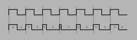
The figure below shows the standard square wave clock, with the 50% duty cycle (half on, half off). Below is an exaggerated pulse width modulated square wave, where we have segmented the period into 8 parts. You can see that the duty cycle is changing linearly (only part of the full modulation is shown). Note that the period of the PWM wave is still the same, and the posedge lines line up with the 50-50 square wave. For PWM, it's the duty cycle that changes, not the period.
The Vivado project for this PWM can be downloaded here.
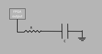
That the led takes time to turn on suggests that it has some capacitance, which suggests that we could construct a (somewhat primitive) waveform generator using a real capacitor and resistor, taking advantage of the finite (and known) capacitance and the PWM.
The circuit will look something like this:
Using the FSM above, this means that we will have a pulse that has a period T=10ns× 211=20.48μs. If we modulate that pulse up and down, it will take 2 cycles of 11 bits each (1 11 bit cycle to go from 0 to 100% duty factor, and another to go from 100% to 0). We also have a counter that determines how long the particular duty cycle is constant (n bits). So the wave period that will come out of this will be Tw = T × 2× 211 ċ 2n = 0.08 × 2n. If we set n=4, then the wave will have a period of Tw = 1.34s, which seems good enough.
The following codes implements the above. Note that in the code, you can see several outputs: the modulated pulse width output of the FPGA will come out of JA, pin 1 and pin 2 (so that you can see the pulse on a scope and at the same time send it to the breadboard and through the RC circuit). We also use the bottom 5 switches to control the time that the duty cycle is constant (the counter mentioned in the paragraph above): counter will be set to whatever value is on the switches, except if all 5 switches are set to 0, in which case the counter will be set to the maximum 5'h1F.
`timescale 1ns / 1ps

module top(
    input clk,
    input [15:0] sw,
    input btnU,             // reset
    output [15:0] led,
    output wave,            // this drives the RC circuit and is same as OUT
    output wave2,           // also same as OUT but free of RC circuit
    output reg pulse,        //
    output reg count_down    // 0=increment, 1=decrement
    );

    //
    // turn the FSM on using sw[15];
    //
    wire enable = sw[15];
    //
    // let's say we want 1024 times the clock period for period of the output signal
    //
    // for the "on" and "off" registers, we will modulate them using a large register.
    // so full scale 100% duty factor will be ON='h3FF and OFF = 0, so the calculation
    // we need is:
    //
    //
    // now make the counters and the output and the FSM
    //
    reg [10:0] count_on, count_off;
    reg [10:0] on, off;
    wire [10:0] width_on, width_off;
    parameter [10:0] FULL = 11'h7FE;
    parameter [10:0] START = 11'h001;
    reg OUT;
    reg [4:0] change_width;
    //
    // "beats" is the value of the counter that determines how long the duty cycle
    // is constant
    //
    wire [4:0] sw8 = sw[4:0];
    wire [4:0] beats = (sw8 == 5'h0 ? 5'h1F : sw8);
    localparam [1:0] WAIT=0, ON=1, OFF=2, CHANGE=3;
    reg [1:0] state;
    always @ (posedge clk)
        if (btnU) begin
            state <= WAIT;
            OUT <= 0;
            on <= START;
            off <= FULL;
            change_width <= 0;
            count_down <= 0;
            pulse <= 0;
        end
        else case (state)
            WAIT: begin
                OUT <= 0;
                count_on <= 0;
                count_off <= 0;
                on <= START;
                off <= FULL;
                count_down <= 0;
                change_width <= 0;
                pulse <= 0;
                if (enable) state <= ON;
                else state <= WAIT;
            end
            ON: begin
                OUT <= 1;
                count_off <= 0;
                count_on <= count_on + 1;
                if (count_on == on) state <= OFF;
                else state <= ON;
            end
            OFF: begin
                OUT <= 0;
                count_on <= 0;
                count_off <= count_off + 1;
                if (count_off == off) state <= CHANGE;
                else state <= OFF;
            end
            CHANGE: begin
                //
                // in this state we check to see if it's time to change the on/off percentage
                //
                change_width <= change_width + 1;
                if (change_width == beats) begin
                    change_width <= 0;
                    if (count_down) begin
                        on <= on - 1;
                        off <= off + 1;
                        if (on == START) begin
                            pulse = ~pulse;
                            count_down <= 0;
                        end
                    end
                    else begin
                        on <= on + 1;
                        off <= off - 1;
                        if (on == FULL) count_down <= 1;
                    end
                 end
                 if (enable) state <= ON;
                 else state <= WAIT;
            end
            default: begin
                count_on <= 0;
                count_off <= 0;
                on <= 0;
                count_down <= 0;
                change_width <= 0;
                state <= WAIT;
            end
        endcase
    //
    // now drive the output onto led[15]
    //
    assign led = {OUT,9'h0,on[5:0]};
    assign wave = OUT;
    assign wave2 = OUT;
endmodule
The pinouts (.xdc file) will look like this:
## This file is a general .xdc for the Basys3 rev B board
## To use it in a project:
## - uncomment the lines corresponding to used pins
## - rename the used ports (in each line, after get_ports) according to the top level signal names in the project

## Clock signal
set_property PACKAGE_PIN W5 [get_ports clk]
set_property IOSTANDARD LVCMOS33 [get_ports clk]
create_clock -period 10.000 -name sys_clk_pin -waveform {0.000 5.000} -add [get_ports clk]

# wave output
set_property PACKAGE_PIN J1 [get_ports wave]
set_property IOSTANDARD LVCMOS33 [get_ports wave]
set_property PACKAGE_PIN L2 [get_ports wave2]
set_property IOSTANDARD LVCMOS33 [get_ports wave2]
set_property PACKAGE_PIN J2 [get_ports pulse]
set_property IOSTANDARD LVCMOS33 [get_ports pulse]
set_property PACKAGE_PIN G2 [get_ports count_down]
set_property IOSTANDARD LVCMOS33 [get_ports count_down]


# LEDs
set_property PACKAGE_PIN U16 [get_ports {led[0]}]
set_property IOSTANDARD LVCMOS33 [get_ports {led[0]}]
set_property PACKAGE_PIN E19 [get_ports {led[1]}]
set_property IOSTANDARD LVCMOS33 [get_ports {led[1]}]
set_property PACKAGE_PIN U19 [get_ports {led[2]}]
set_property IOSTANDARD LVCMOS33 [get_ports {led[2]}]
set_property PACKAGE_PIN V19 [get_ports {led[3]}]
set_property IOSTANDARD LVCMOS33 [get_ports {led[3]}]
set_property PACKAGE_PIN W18 [get_ports {led[4]}]
set_property IOSTANDARD LVCMOS33 [get_ports {led[4]}]
set_property PACKAGE_PIN U15 [get_ports {led[5]}]
set_property IOSTANDARD LVCMOS33 [get_ports {led[5]}]
set_property PACKAGE_PIN U14 [get_ports {led[6]}]
set_property IOSTANDARD LVCMOS33 [get_ports {led[6]}]
set_property PACKAGE_PIN V14 [get_ports {led[7]}]
set_property IOSTANDARD LVCMOS33 [get_ports {led[7]}]
set_property PACKAGE_PIN V13 [get_ports {led[8]}]
set_property IOSTANDARD LVCMOS33 [get_ports {led[8]}]
set_property PACKAGE_PIN V3 [get_ports {led[9]}]
set_property IOSTANDARD LVCMOS33 [get_ports {led[9]}]
set_property PACKAGE_PIN W3 [get_ports {led[10]}]
set_property IOSTANDARD LVCMOS33 [get_ports {led[10]}]
set_property PACKAGE_PIN U3 [get_ports {led[11]}]
set_property IOSTANDARD LVCMOS33 [get_ports {led[11]}]
set_property PACKAGE_PIN P3 [get_ports {led[12]}]
set_property IOSTANDARD LVCMOS33 [get_ports {led[12]}]
set_property PACKAGE_PIN N3 [get_ports {led[13]}]
set_property IOSTANDARD LVCMOS33 [get_ports {led[13]}]
set_property PACKAGE_PIN P1 [get_ports {led[14]}]
set_property IOSTANDARD LVCMOS33 [get_ports {led[14]}]
set_property PACKAGE_PIN L1 [get_ports {led[15]}]
set_property IOSTANDARD LVCMOS33 [get_ports {led[15]}]

## Switches
set_property PACKAGE_PIN V17 [get_ports {sw[0]}]
set_property IOSTANDARD LVCMOS33 [get_ports {sw[0]}]
set_property PACKAGE_PIN V16 [get_ports {sw[1]}]
set_property IOSTANDARD LVCMOS33 [get_ports {sw[1]}]
set_property PACKAGE_PIN W16 [get_ports {sw[2]}]
set_property IOSTANDARD LVCMOS33 [get_ports {sw[2]}]
set_property PACKAGE_PIN W17 [get_ports {sw[3]}]
set_property IOSTANDARD LVCMOS33 [get_ports {sw[3]}]
set_property PACKAGE_PIN W15 [get_ports {sw[4]}]
set_property IOSTANDARD LVCMOS33 [get_ports {sw[4]}]
set_property PACKAGE_PIN V15 [get_ports {sw[5]}]
set_property IOSTANDARD LVCMOS33 [get_ports {sw[5]}]
set_property PACKAGE_PIN W14 [get_ports {sw[6]}]
set_property IOSTANDARD LVCMOS33 [get_ports {sw[6]}]
set_property PACKAGE_PIN W13 [get_ports {sw[7]}]
set_property IOSTANDARD LVCMOS33 [get_ports {sw[7]}]
set_property PACKAGE_PIN V2 [get_ports {sw[8]}]
set_property IOSTANDARD LVCMOS33 [get_ports {sw[8]}]
set_property PACKAGE_PIN T3 [get_ports {sw[9]}]
set_property IOSTANDARD LVCMOS33 [get_ports {sw[9]}]
set_property PACKAGE_PIN T2 [get_ports {sw[10]}]
set_property IOSTANDARD LVCMOS33 [get_ports {sw[10]}]
set_property PACKAGE_PIN R3 [get_ports {sw[11]}]
set_property IOSTANDARD LVCMOS33 [get_ports {sw[11]}]
set_property PACKAGE_PIN W2 [get_ports {sw[12]}]
set_property IOSTANDARD LVCMOS33 [get_ports {sw[12]}]
set_property PACKAGE_PIN U1 [get_ports {sw[13]}]
set_property IOSTANDARD LVCMOS33 [get_ports {sw[13]}]
set_property PACKAGE_PIN T1 [get_ports {sw[14]}]
set_property IOSTANDARD LVCMOS33 [get_ports {sw[14]}]
set_property PACKAGE_PIN R2 [get_ports {sw[15]}]
set_property IOSTANDARD LVCMOS33 [get_ports {sw[15]}]

##Buttons
set_property PACKAGE_PIN T18 [get_ports btnU]
set_property IOSTANDARD LVCMOS33 [get_ports btnU]
The full archived project can be found
here.
The signals are brought out and connected to the RC circuit, and one of the SALEAE logic analyzers that can show both analog and digital pulses. The waveform is shown below:
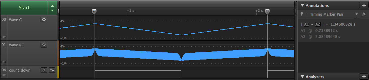
The top trace, "Wave C", shows the analog voltage across the capacitor C. The next trace, called "Wave RC" shows the voltage across the RC, and the bottom trace is count_down. There's a ground pin on the logic analyzer, connected to the BASYS3 ground. The wave "Wave RC" shows the voltage across the circuit, complete with all of the high frequency components. "Wave C" shows the voltage across the capacitor, which is effectively a high pass device, pushing all of the AC components through it leaving the DC components. Hence a nice triangle wave. If we set the switches to 01111 (first 4 from the right are on, the 5th is off), then we measure the period of the triangle wave to be approximately 1.34s as expected.
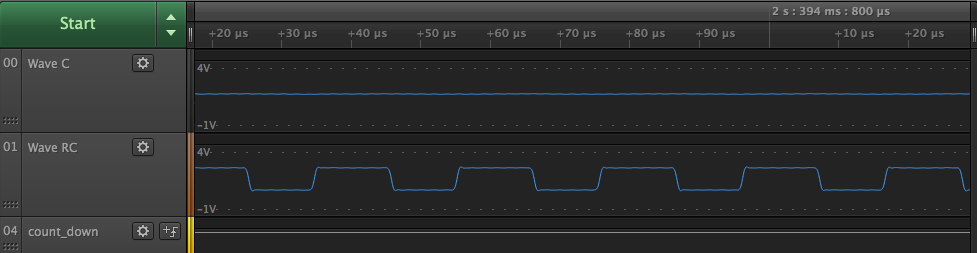
To see the AC component across "Wave RC", we can blow up the logic analyzer picture, as in the following figure. You can see that "Wave RC" is oscillating around some nonzero DC level. This is the oscillation that is filtered out when you just look at the voltage across the capacitor.
Note that you have to take care not to try to use the logic analyzer to look at the voltage across the resistor by putting a ground (return) between the R and C component, as in the circuit above, or you will be drawing current into the logic analyzer ground.
This is how you can build a waveform generator, however you would also have to have various capacitors for the different scales if you want to have various decades of frequencies.