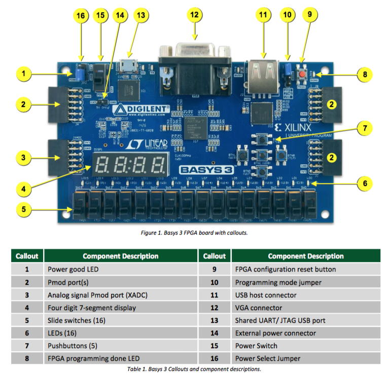
The BASYS3 board has, in addition to the push buttons, switches, and LEDs, 4 rectangular connectors called "PMOD connectors". These are shown as items 2 and 3 in the figure on page 2 of basys3_rm.pdf, or in the figure below:
The 3 connectors labeled "2"
are general purpose
digital IO blocks that can be used for any kind of IO supported by
the FPGA (even differential). The connector labeled "3" can be used
for either digital or analog signals that are digitized inside the FPGA.
Page 17 of basys3_rm.pdf details how
to use the digital IO blocks. The 3 "PMOD" connectors are labeled
either "JA" (upper left), "JB" (upper right), or "JC" (lower right),
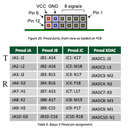
and all conform to the following diagram (also on page 17):
If you look on the BASYS3 board itself, you will see clearly the
label (JA, etc) and where the pin labeled 1 starts: it is always
on the top on one edge, whereas the 3V output is pin 6 on the other
side on the top. All you have to do is route your digital signals
into the right input and connect the port to the FPGA in the
xdc file. For example, the diagram shows that for JA, pin 1
(labeled "JA1") is connected to pin "J1" on the FPGA. That means
you have to specify "J1" in the .xdc file. The following is an
example of connecting all pins in JA to the FPGA and referring
to them in the top level verilog file as an 8-bit bus called
"JA". The xdc code looks like this:
and the verilog input looks like this:
LVDS is a low voltage differential standard that is very commonly
used. Wikipedia has a pretty good page explaining it
here, but basically instead of switching voltage on a single
wire, in LVDS you switch a small amount of current, nominally
3.5mA. The thing is differential, and you have to terminate by putting
a resistor across the inputs usually. The voltage swing is around
800mV, so if you terminate the far end of the differential cable with
$100\Omega$, then you will draw 8mA of current.
Outputing a digital 1 means 8mA of current goes from plus to minus,
and vice versa for a digital 0.
On modern FPGAs, like the Artix7 in the BASYS3 board, the IO pins
can be configured for a host of different IO standards, but for
differential signals, they specify which pins are "paired".
This information is sometimes difficult to find, so it is
provided in the txt mapping file
here. You have to search
for the pins that are paired and set things correctly in the
.xdc file. For instance, say you want to input a differential
signal into the BASYS3 on JA using pin 1 and another pin.
Pin 1 is JA1 in the diagram, and that's pin "J1". In the
above file, you look for "J1" in the left column, and it is
found on line 116:
The pin name is "IO_L3N_T0_DQS_AD5N_35", so you search for the
pair with the name "IO_L3P_T0_DQS_AD5N_35" (note the difference,
"IO_L3N..." and "IO_L3P...") and you can see that that's on pin
"H1", right above (line 115), and "H1" is tied to "JA7", which
is pin 7 on connector JA, which is right below "JA1". No
coincidence! That makes it easy to drive a differential pair
in this block.
In the .xdc file you add something like the following for those 2 pins:
The IO standard is 2.5V, and the port name will be "lvds1_p" and
"lvds1_n". In your toplevel verilog, you would then add the
following to turn that into a single ended digital signal that
you can use in the code:
The Artix7 FPGA version on the BASYS3 board (XC7A35T) contains analog-to-digital
(ADC) circuitry that allows it to monitor various temperatures, voltages, and
other things needed to know how the chip is working. You can access this
circuitry to input an analog voltage, either directly through dedicated analog
input pints, or through IO pins that can be used for either analog or digital.
The ADC circuitry is extremely complex, but for simple slowly changing analog
signals, is extremely useful. The technical details are patented, and Xilinx
is not keen on disclosing, however it is described in some detail in a
Google Patent here (but good luck
in digging out too much details, it is a patent so difficult to read). The
circuitry is available in many of the Xilinx chips other than Artix7, and is
called an "XADC" block.
The Artix7 we are using contains 1 XADC block,
which has 2 12-bit 1 MSPS (mega samples per second) ADCs, and an on-chip
analog multiplexer so that you can route 17 different inputs into the ADC.
The amplifiers support unipolar, bipolar, and differential inputs. For
more technical information on how to use it, see the Xilinx app note
ug480_7Series_XADC.pdf.
These ADCs can be used for various things like temperature monitoring,
or even DAQ for externally driven circuits. In fact, if you don't use
the ADC in your design, it then automatically digitizes all on-chip
sensors for readout over the serial JTAG interface (this is described in
the above document). The internal XADC can convert signals from:
The JXADC header is the one next to the 4 digit display,
and they are paired (positive/negative)
such that the positive pin is on the top row and the negative pin is on the
bottom row in the same column.
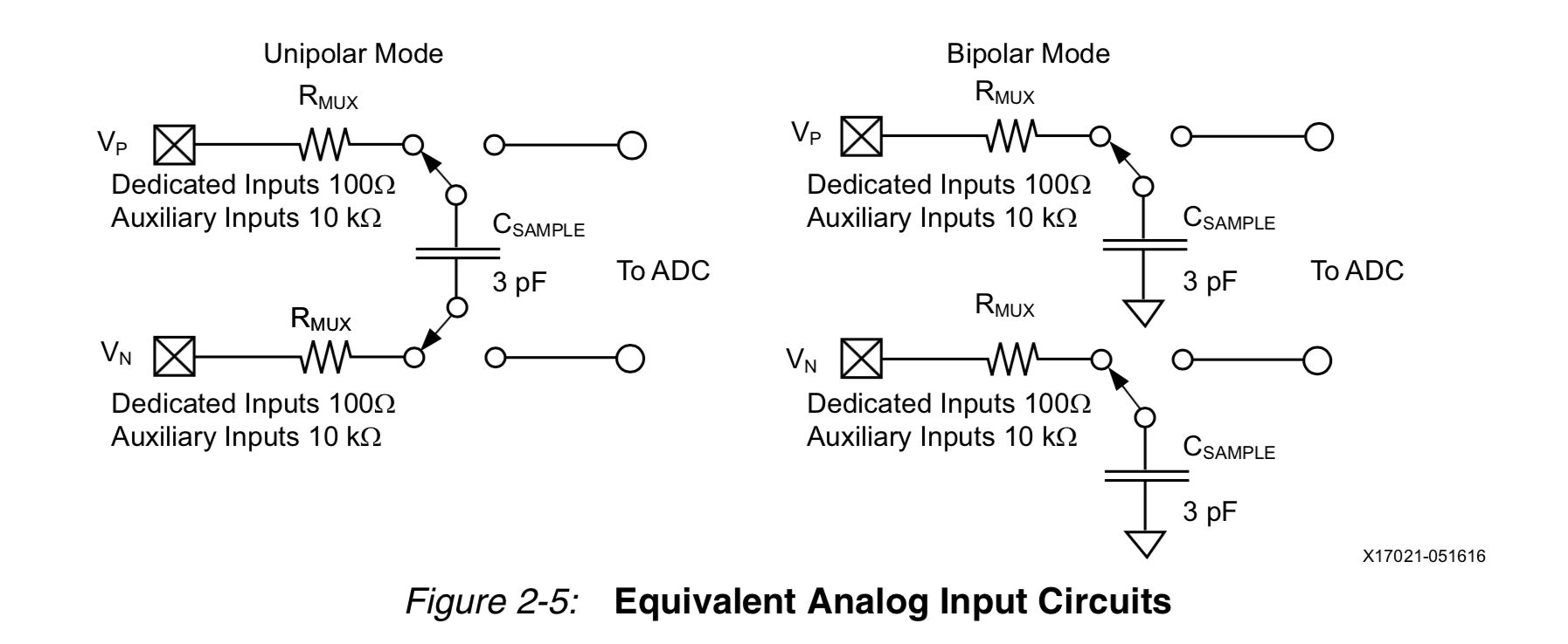
The XADC can measure unipolar ($0\to 1$ volt) or bipolar ($-0.5\to +0.5$ volt) signals.
The figure below comes from page 30 of the
XADC manual):
We will be using unipolar mode, and the BASYS3 board only wires up the
dual analog/digital inputs to the FPGA, so we will only be using the
"VAUX" inputs. That means that the input impedance of our XADC will
be around $10k\Omega$, and the sampling capacitor will be around $3pF$,
giving an RC chargeup time of around $30ns$. Note that in unipolar mode, there are 2
switches that connect the positive and negative sides of the sampling capacitor to the
inputs. They are labeled $V_p$ and $V_n$, which are the dedicated analog inputs,
but it is the same for the "VAUX" inputs that we will use via "JXADC" header.
The way the XADC works is typical of analog-to-digital conversion circuits.
A "sample and hold" capacitor is charged up by virtue of an incoming voltage
signal, and this is usually gated so that you can control when it charges.
Charging is the "sample" phase.
Once it is charged, it is disconnected from the inputs, and the voltage will
hold while the signal is being converted from a voltage into a digital
number. This is the "hold" phase. Ideally you want the capacitor to be
small enough so that it charges up fast, but not too small such that any
stray capacitance can compete. And you want the input impedance to be such
that the RC time for charging ($\tau = RC$) is small. Often you will see
ADCs that first charge, and then hold and convert, doing them serially,
which puts a big burden on the front-end analog circuitry to charge up
quickly (so that the overall data rate can be large).
What the Xilinx XADC
does, instead, is to have two sample and hold capacitors like in the figure.
So the XADC can sample and convert simultaneously.
The ADC itself is 12 bits. This means there are $2^{12}=4096$ possible
values, and since the maximum voltage is $1.0$ volts, that means that
the LSB is $1/2^{12}=0.244$mV, which means the precision is around
half that, or $\delta V = 0.122$mV. The rise time of the voltage on the sampling
capacitor is given by $\tau = RC = 30ns$, which means that the voltage
on the capacitor $V_c$ increases with time according to:
$$V_c = V_{in}(1-e^{-t/\tau})\nonumber$$
If $V_{in}$ is the maximum $1.0$ volts, then we can calculate the
time $t_{\delta}$ (or the number of RC times $N\tau$) that
it will take for the signal to get to within $\delta V$ of $V_{in}$, so
that the charging does not dominate the precision:
$$V_{\delta}=V_{in}(1-\delta V)=V_{in}(1-e^{-N})\nonumber$$
which means $\delta V=e^{-t_{\delta}/\tau}$, and solving for $t_{\delta}$
gives
$$N\tau = -\tau\ln\delta V = 9.01\tau\nonumber$$
For $\tau=30ns$, that means we would need around $270ns$ of charging
so that our precision is not dominated by the charging time. The XADC
will run at 1M samples per second (1 MSPS), or $1\mu s$, with parallel
sampling and conversion, so charging will not be a problem, but you should
keep this precision in mind in case you use it at a slower sampling rate.
Using the XADC with VAUX inputs to measure voltages that change on a time
scale longer than the $1\mu s$ operation time will work great, even if we
are not controlling the conversion with a "trigger", something that synchronizes
conversion with the incoming signal. However, if you want to use the XADC
to measure voltages that are changing fast with respect to $1\mu s$, you have
to build a preamp that will integrate the signal using a differential
amplifier with a capacitor as feedback. This is the subject of another
course.
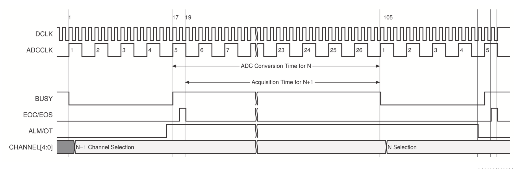
The figure below details the timing of the XADC internals:
A full cycle of conversion takes 26 ticks of the internal clock called ADCCLK, which is derived
from the input clock .dclk_in. Setting configuration register 2 allows you
to determine the ADCCLK frequency.
The documentation is a bit fuzzy, but there was a
technical note
that says the ADCCLK has to be between 1 and 26 MHz if you want to run the ADC at the maximum
1 Msps conversion. For our purposes, we will use the on board 100MHz clock, divide
it in half to get 50MHz, and use that as
input .dclk_in, so our divider will be 2 (see table above), and we will have a 25MHz
ADCCLK which will set the conversion rate to $R=25/26=961.5$ksps.
By using a 50MHz .dclk_in, some of the timing pulses (described below) will be
~20ns wide, which means we can use the 100MHz clock to run state machines and branch
on pulses without encountering race conditions (this is probably overly cautious!).
The conversion period includes all of the time it
takes to assemble and latch the output bits so that they become available
to be latched inside the FPGA by your code.
A good reference for different ways to use the XADC is available
here.
The ADC allows 4 ticks for the capacitor to fully charge and settle,
and can be increased to 10 (see documentation). There are 2
sample-and-hold capacitors, so that one can be charging up
while the other is being digitized.
As you can see in the diagram, .eoc_out is asserted on every conversion,
so the .eoc_out for channel "N-1" in the diagram is the second one asserted
in the diagram, which happens when channel "N" is being converted. Below we
show the logic analyzer output for the XADC.
The ADC on the Artix7 can be configured so that you can trigger it from an
event, or you can enable it by controlling the input enable (.den_in,
short for "data enable in"),
or you can just let it run free and keep digitizing the analog signal you
are sending it by tying the .eoc_out signal, which is a 1 clock tick signal
meaning "end of conversion", to the .den_in signal. This is how we will use
it to build the voltmeter.
A caveat is that if the signal is rising during the time you are digitizing,
you might not get the full value of the voltage, but if your voltage is DC
(or changing slow compared to $1\mu s$) then you won't notice this.
If your signal has a significant AC component however, this can be handled by using the
XADC in event mode instead of the continuous mode that we will be using.
All of this is detailed starting on page 73 of the
XADC manual.
The input voltage to be converted has to be between 0 and 1.0 volts (for
unipolar mode), and the ADC produces a 12 bit number in the upper 12 bits
of the .do-out bus. The resolution of a single bit (LSB) is therefore
$\delta = 1V/1^{12}=244\mu V$. Bipolar mode is more complex and won't be
used here.
The hard part in setting this up is in generating an instantiation of
the XADC into your verilog code.
You can go ahead and do it by hand by
clicking on "Language Templates" under "PROJECT MANAGER", then
click on "Verilog/Device Primitive Instantiation/Artix-7Advanced" and
you will see "Xilinx Analog-to-Digital Converter (XADC)". If you
click on that you will see an example instantation in the right panel.
Cut and paste to your top level file.
However, you will find that for complicated things like XADC, it is
often better to run a "Wizard" and let Xilinx do it for you. This is
the approach we will take here.
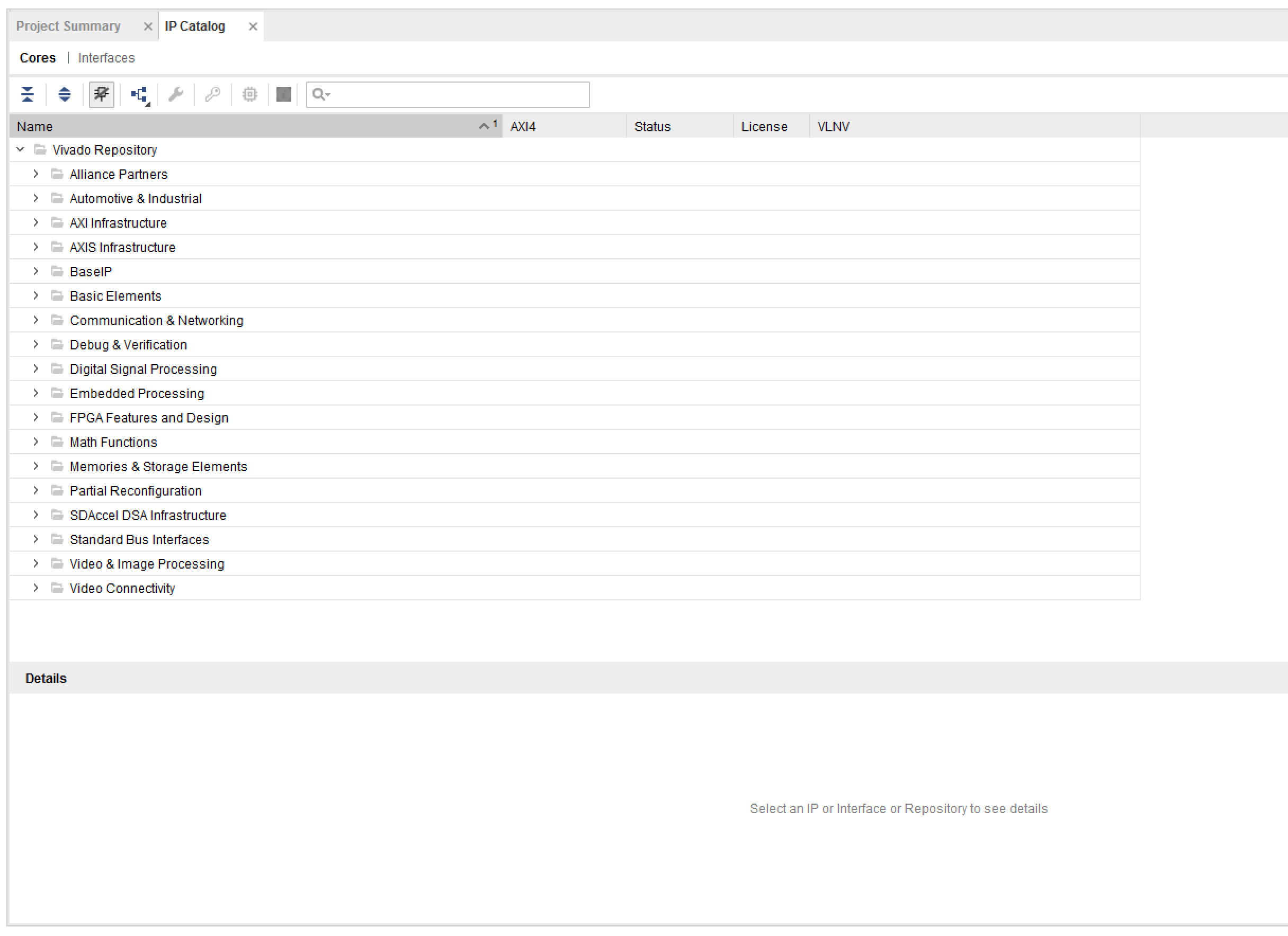
To start, click on "IP Catalog" under "PROJECT MANAGER" in the
left panel. It will bring up a new window in one of your panels,
with a tab labeled "IP Catalog". It will look something like this:
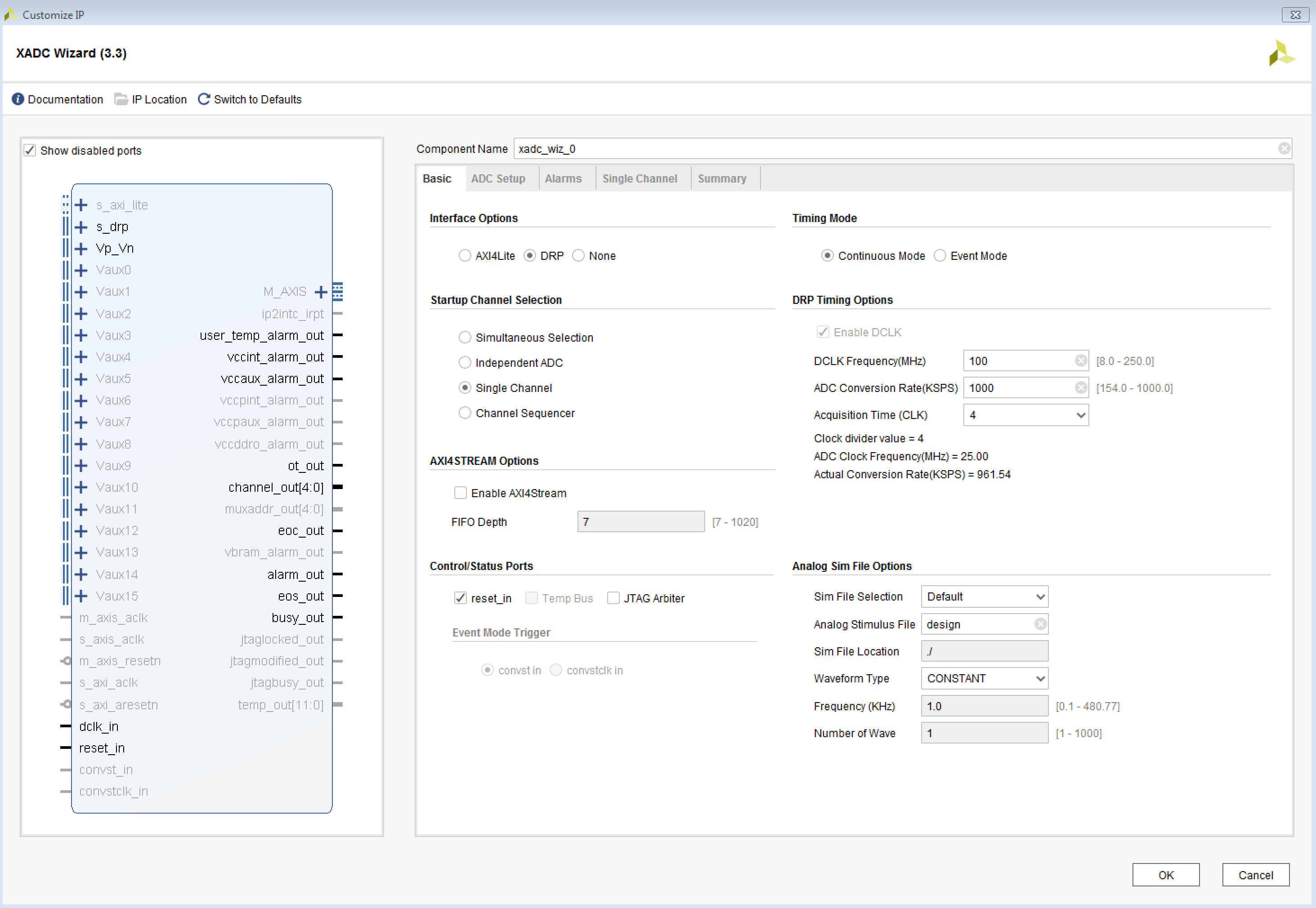
Type XADC into the search window, and it should find the "XACD Wizard".
Double click and it will run the wizard, you should see something
like this to begin:
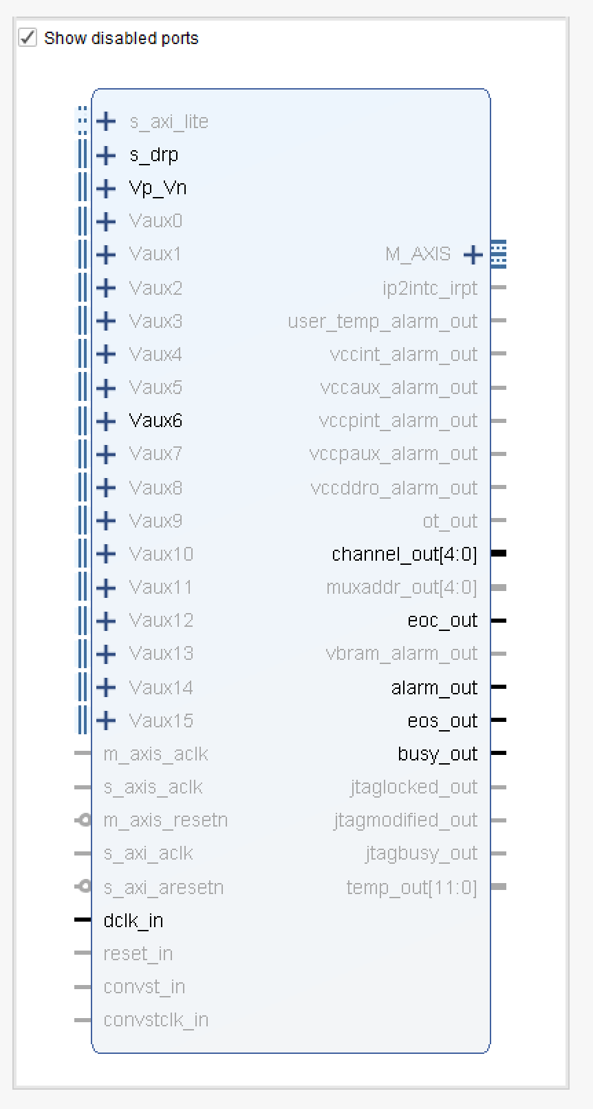
You will see a text field called "Component Name" and you will see
"xadc_wiz_0" in that field. That's fine, it is just the instantiation
name, and will show up with this name in your verilog sources panel.
Underneath "Component Name" you will see 5 tabs labeled "Basic",
"ADC Setup", "Alarms", "Single Channel", and "Summary", and these
are used to set up the instantiation. Here's what
is recommended for each of these tabs:
Click "OK", and you should see a popup window that asks if it's ok to
create a new directory to house all of the new files. It should be
in your project directory. Click "OK". It will then pop up a window
labeled "Generate Output Product". Click "Generate", it will initiate
some activity, and at the end will inform you that it did what it was
supposed to do. Click OK.
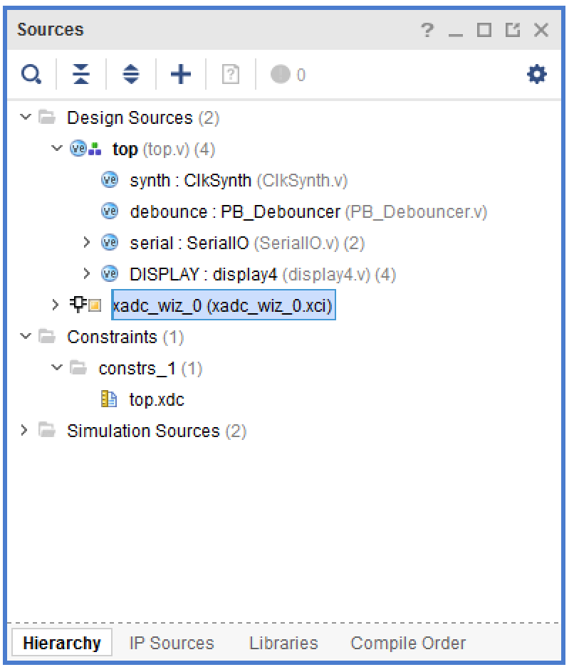
Now you should see a new source appear in the same panel with the other
sources, and it should look something like this:
If you open up what's below "xadc_wiz_0" you should see a file called
"xadc_wiz_0 (xadc_wiz_0.v)". That's your source file, it contains
the instantiation of the XADC. You can double click on it, and you will
a huge number of lines. Don't worry, all we have to do now is
instantiate xacd_wiz_0 and that module will do all the heavy lifting.
To instantiate you should place the following template in your code:
This instantiation will produce a series of configuration registers that
control how the XADC works. The configuration registers can be written to
and read from using the DRP (Dynamic Reconfiguration Port), which we will not
use. But it's good to see how these registers are configured, as depicted
in the list below (which comes from the verilog instantiation):
Digital IO
##Pmod Header JA
##Sch name = JA1
set_property PACKAGE_PIN J1 [get_ports {JA[0]}]
set_property IOSTANDARD LVCMOS33 [get_ports {JA[0]}]
##Sch name = JA2
set_property PACKAGE_PIN L2 [get_ports {JA[1]}]
set_property IOSTANDARD LVCMOS33 [get_ports {JA[1]}]
##Sch name = JA3
set_property PACKAGE_PIN J2 [get_ports {JA[2]}]
set_property IOSTANDARD LVCMOS33 [get_ports {JA[2]}]
##Sch name = JA4
set_property PACKAGE_PIN G2 [get_ports {JA[3]}]
set_property IOSTANDARD LVCMOS33 [get_ports {JA[3]}]
##Sch name = JA7
set_property PACKAGE_PIN H1 [get_ports {JA[4]}]
set_property IOSTANDARD LVCMOS33 [get_ports {JA[4]}]
##Sch name = JA8
set_property PACKAGE_PIN K2 [get_ports {JA[5]}]
set_property IOSTANDARD LVCMOS33 [get_ports {JA[5]}]
##Sch name = JA9
set_property PACKAGE_PIN H2 [get_ports {JA[6]}]
set_property IOSTANDARD LVCMOS33 [get_ports {JA[6]}]
##Sch name = JA10
set_property PACKAGE_PIN G3 [get_ports {JA[7]}]
set_property IOSTANDARD LVCMOS33 [get_ports {JA[7]}]
    .
    .
    .
    input [7:0] JA,
    .
    .
    .
The .xdc file specifies the i/o standard as "LVCMOS33",
which just means that it expects the signal to go between
0 volts (digital 0) and 3.3 volts (digital 1). Other
standards are of course possible.
LVDS Input
J1 IO_L3N_T0_DQS_AD5N_35 ....
set_property PACKAGE_PIN H1 [get_ports lvds1_p ]
set_property IOSTANDARD LVDS_25 [get_ports lvds1_p ]
set_property PACKAGE_PIN J1 [get_ports lvds1_n ]
set_property IOSTANDARD LVDS_25 [get_ports lvds1_n ]
    module .... (
        .
        .
        .
        input lvds1_p, lvds1_n,   // Pmod JA, 1 (J1) and 7 (H1) right most pair top and bottom of connector
        .
        .
        .
    );
    .
    .
    .
    wire single_ended;
    IBUFDS dif2single1 (.I(lvds1_p), .IB(lvds1_n), .O(single_ended) );
    .
    .
    .
The IBUFDS instantiation is an internal Xilinx "primitive" that they
provide, so all you have to do is refer to it correctly. It will take
the 2 differential inputs and turn them into a single ended signal that
you can use.
Analog IO
CPG236 Name Artix7 pin BASYS3 JXADC Pin
IO_L7P_T1_AD6P_35 J3 1
IO_L7N_T1_AD6N_35 K3 7
IO_L8P_T1_AD14P_35 L3 2
IO_L8N_T1_AD14N_35 M3 8
IO_L9P_T1_DQS_AD7P_35 M2 3
IO_L9N_T1_DQS_AD7N_35 M1 9
IO_L10P_T1_AD15P_35 N2 4
IO_L10N_T1_AD15N_35 N1 10
Xilinx XADC
Xilinx XADC Timing
XADC Instantiation Using IP Wizard
Now you are ready to generate the instantiation. You will see in the
left panel what pins will be driven, it should look like this:
    xadc_wiz_0 XADC_INST (
        .daddr_in(daddr_in[6:0]),
        .dclk_in(dclk_in),
        .den_in(den_in),
        .di_in(di_in[15:0]),
        .dwe_in(dwe_in),
        .vauxp6(vauxp6),
        .vauxn6(vauxn6),
        .busy_out(busy_out),
        .channel_out(channel_out[4:0]),
        .do_out(do_out[15:0]),
        .drdy_out(drdy_out),
        .eoc_out(eoc_out),
        .eos_out(eos_out),
        .alarm_out(alarm_out),
        .vp_in(vp_in),
        .vn_in(vn_in)
    );
Here's what you do with each of these ports:
        .INIT_40(16'h0016), // config reg 0
        .INIT_41(16'h31AF), // config reg 1
        .INIT_42(16'h0200), // config reg 2
        .INIT_48(16'h0100), // Sequencer channel selection
        .INIT_49(16'h0000), // Sequencer channel selection
        .INIT_4A(16'h0000), // Sequencer Average selection
        .INIT_4B(16'h0000), // Sequencer Average selection
        .INIT_4C(16'h0000), // Sequencer Bipolar selection
        .INIT_4D(16'h0000), // Sequencer Bipolar selection
        .INIT_4E(16'h0000), // Sequencer Acq time selection
        .INIT_4F(16'h0000), // Sequencer Acq time selection
        .INIT_50(16'hB5ED), // Temp alarm trigger
        .INIT_51(16'h57E4), // Vccint upper alarm limit
        .INIT_52(16'hA147), // Vccaux upper alarm limit
        .INIT_53(16'hCA33),  // Temp alarm OT upper
        .INIT_54(16'hA93A), // Temp alarm reset
        .INIT_55(16'h52C6), // Vccint lower alarm limit
        .INIT_56(16'h9555), // Vccaux lower alarm limit
        .INIT_57(16'hAE4E),  // Temp alarm OT reset
        .INIT_58(16'h5999), // VCCBRAM upper alarm limit
        .INIT_5C(16'h5111),  //  VCCBRAM lower alarm limit
The following table summarizes the configuration registers. For our purposes, since we are running in continuous single channel mode and no alarms, only the configuration registers are important.
Register (hex) Value
Name Comments
40 'h0016 config reg 0
4:0 selects ADC input channels, 16 means VAUX 6 only.
Settling time is 4 ticks, continuous mode,
unipolar, no external multiplexer mode,
and use averaging to calculate calibration coefficients.
41 'h31AF config reg 1
disable temperature alarms, enable ADC gain corrections, disable offset
corrections, set single channel mode
42 'h0200 config reg 2
ADCCLK = dclk_in divided by x2
All rights reserved. No part of this publication may be reproduced, distributed, or transmitted in any
form or by any means, including photocopying, recording, or other electronic or mechanical methods, without
prior written permission, except in the case of brief quotations embodied in critical
reviews and certain other noncommercial uses permitted by copyright law.
Unless indicated otherwise, any lecture handouts, exams, homework and exam solutions,
and the lectures themselves (including audio and video recordings) are copyrighted by
me and may not be distributed or reproduced for anything other than your personal use
without my written permission.
Last updated October, 2023 Drew Baden