|
Introduction to Carbon
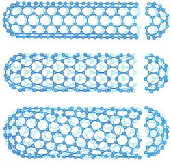
Nanotubes Understanding the electronic properties of the graphene sheet helps to understand the electronic properties of carbon nanotubes. Graphene is a zero-gap semiconductor; for most directions in the graphene sheet, there is a bandgap, and electrons are not free to flow along those directions unless they are given extra energy. However, in certain special directions graphene is metallic, and electrons flow easily along those directions. This property is not obvious in bulk graphite, since there is always a conducting metallic path which can connect any two points, and hence graphite conducts electricity. However, when graphene is rolled up to make the nanotube, a special direction is selected, the direction along the axis of the nanotube. Sometimes this is a metallic direction, and sometimes it is semiconducting, so some nanotubes are metals, and others are semiconductors. Since both metals and semiconductors can be made from the same all-carbon system, nanotubes are ideal candidates for molecular electronics technologies.
In addition to their interesting electronic structure, nanotubes have a number of other useful properties. Nanotubes are incredibly stiff and tough mechanically - the world's strongest fibers. Nanotubes conduct heat as well as diamond at room temperature. Nanotubes are very sharp, and thus can be used as probe tips for scanning-probe microscopes, and field-emission electron sources for lamps and displays. Device Fabrication Find 'em and wire 'em
The disadvantages of the find
'em and wire 'em scheme are that we are able to make only a limited
number of devices, and the technique is not "scalable"
- that is, making twice as many devices takes twice as much time.
If nanotubes are to find electronic applications in industry, scalable
fabrication techniques will be needed. However, our current techniques
allow us to jump ahead and explore single nanotube devices, to see
if they have the useful properties that would warrant developing
techniques to mass produce devices. CVD growth of nanotubes
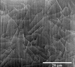
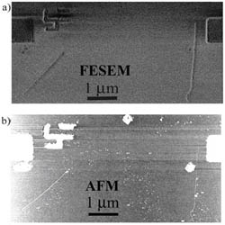
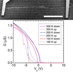
Typically we use silicon chips (pieces of flat silicon wafer from the semiconductor industry) as our substrate material, with a layer of silicon dioxide (glass) grown on top of the silicon as an insulator. The catalyst con be obtained in several ways; the easiest is to dip the silicon chip into a solution of ferric nitrate in isopropanol, and then dip the chip into hexane to cause the ferric nitrate to come out of solution. This deposits nanocrystals of ferric nitrate on the chip, which can be reduced to iron with hydrogen in the growth furnace. Locating the nanotubes Recently we have developed a technique to image nanotubes using the scanning electron microscope (SEM). This imaging technique relies on the fact that the nanotubes are conducting, and the substrate on which they are lying is insulating. The SEM images by scanning a high-energy beam of electrons over the sample. Secondary electrons generated by the energetic beam are collected and amplified to produce the image signal. When the SEM beam hits an insulator, some electrons stick in the insulator and it becomes negatively charged. When the beam scans over the nanotube, the electrons are free to spread out along the nanotube, and thus the area around the nanotube is less negatively charged. The less negatively charged area allows more electrons from the substrate to escape and be detected, producing a signal when the beam scans across the nanotube. Examples of SEM and AFM images of nanotubes are seen below.
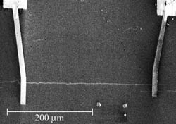
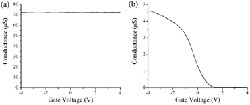
Once the nanotubes are located, they may be contacted electrically using electron-beam lithogrpahy (EBL). A thin layer of resist (a polymer) is spun onto the chip, and the SEM is used again, but this time the energetic electron beam is used to write a pattern in the resist where we want the electrodes to be. The resist which has been exposed to the beam is then washed away in a solvent, and metal (such as gold) is evaporated into the holes in the resist, forming wires which contact the nanotubes. The excess metal which is on top of the resist is lifted off of the chip using a second solvent which dissolves the remaining resist. The electrodes for both the crossed nanotube device and the long nanotube device shown above were fabricated using EBL Electrical measurementsThe wires on the chip are much bigger than the nanotube, but still fairly small - typically the largest parts of the wires on the chip are one or two tenths of a millimeter across. We make contact to the wires on the chip under a microscope, either by using a wire bonder which can attach larger wires to the chip to connect it to a rigid chip holder, or by using a probe station, which has sharp needles that can be used to temporarily make contact to the wires on the chip. Once electrical contacts are made to the nanotubes, we can test their electrical properties. The simplest nanotube device has just two electrode, one at each end of the nanotube. There is actually a third electrode, called the gate, which is the silicon substrate underneath the nanotube. This electrode is not in electrical contact with the nanotube, since it is separated from the nanotube by an insulator (typically silicon dioxide). However, the capacitor formed by the nanotube and the gate can be charged by applying a voltage between nanotube and gate. This way we can change the amount of charge on the nanotube. When we change the gate voltage (changing the amount of charge on the nanotube) and measure the conductance between the two contacts on the nanotube (conductance is the inverse of resistance) we see one of two types of behavior. Either the conductance stays constant as we change the gate voltage, or it drops dramatically as we make the gate voltage more positive (see below). We identify the first type of behavior with the metallic nanotubes - changing the charge on a metal does not change its conductance. The second type of behavior we associate with the semiconducting nanotubes - unless they are "doped", semiconductors don't have any charges which can carry current. The gate voltage allows us to add charge to the nanotube and make it conduct. Negative gate voltage adds "holes" (positive charges corresponding to the absence of an electron) to the nanotube, and it conducts better. Around zero gate voltage there are no holes, and the nanotube stops conducting. (The nanotube should conduct again at a positive enough voltage which would add negatively charged electrons to the nanotube, but it doesn't for reasons related to a barrier at the metal-nanotube interface.)
Conductance and Mobility Recently, much of our research has focused
on semiconducting nanotubes, because of their utility for devices. Since
the conductance of the semiconducting nanotube can be changed by the
voltage on a third electrode (the gate), the nanotube acts like a switch.
This type of switch is called a field-effect transistor (FET), and forms
the basis of most computer chips used today. We are very interested
in determining how well nanotubes perform as field-effect transistors,
in order to gauge their prospects for future electronics applications.
The above analysis also hints that conductivity
isn't the best number to use when comparing one semiconductor to another,
since the conductivity changes with charge density (in this case with
gate voltage). It's fine for metals, like copper, where the charge density
is very high and doesn't change much. The number that's used to indicate
how well one semiconductor conducts compared to another is mobility.
Mobility is the conductance divided by the density of charge carriers,
so it can be used to compare the conductance of semiconductor samples
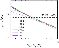
with different amounts of charge to carry the current. We know the charge density in our nanotube devices, because we know the capacitance C between the nanotube and the gate electrode that is producing the charge. The charge Q is proportional to the capacitance and to the amount of gate voltage V we have applied: Q = CV. So we know everything we need to find the mobility. The mobility of one of our long nanotube transistors is shown below.
The mobility is higher than 100,000 cm2/Vs
at room temperature, higher than any other known semiconductor. (The
previous record, for InSb, was 77,000 cm2/Vs, set in 1955.) The mobility
is a function of the gate voltage, and is higher when the gate voltage
is low, i.e. when there are fewer charges in the devices. We don't know
why this is yet, but we are studying this. The mobility is also rather
independent of temperature, suggesting that the thermal vibrations of
the lattice, called phonons, don't play much of a role in scattering
the electrons. |
| Tel: 301.405.3401 1117 Physics Bldg. University of Maryland College Park, MD 20742 |
Contact the
editor. Contact the webmaster. |

 |