A Thinking Person's Guide to Programmable Logic

The basic algebra of binary elements is called Boolean Algebra. As noted in Wikipedia, it is named for George Boole (1815-1864), an English mathematician pioneer in logic. His book "The Laws of Thought" (1854) lays out the algebra of thought, or reasoning.
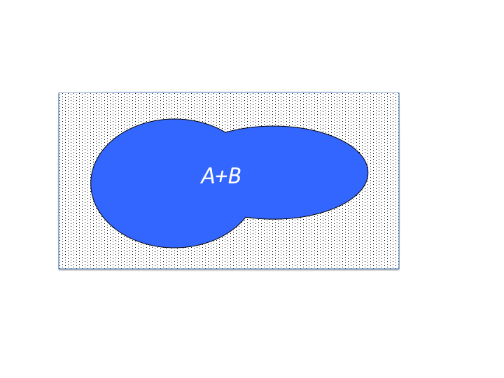
Before getting into the details of Boolean algebra, we can first
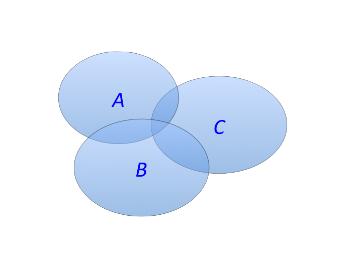
consider a more general visual description of sets and set theory,
and how elements and sets are related. To begin, consider the
following depiction of the "Universe":


So we can write $C=A$ and $B$, or more concisely $C=A\&B$ (and sometimes you will see $C=A\cdot B$), or in the jargon of set theory, $C=A\cap B$, where the symbole $\cap$ means "intersection".
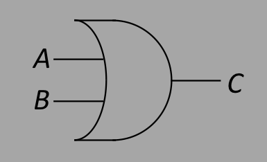
One can also form the "union", or in other words $C=A$ or $B$,
or more commonly $C=A+B$, $C=A|B$, $C=A\cup B$:


| and | or | xor |
|---|---|---|
| $A\cdot B$ | $A+B$ | $A\oplus B$ |
Brief Excursion to Bayesian Statistics | Back to top |
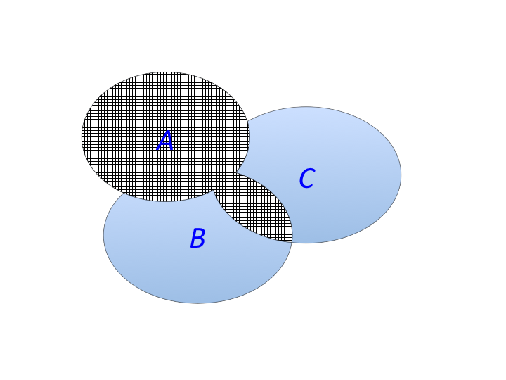
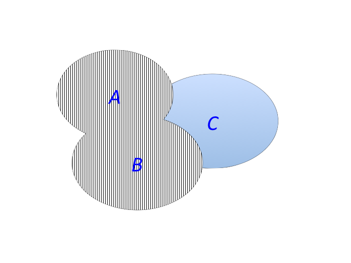
The area $C$ is the intersection of $A$ and $B$, can be written as $A\cap B$, and can be thought of in 2 ways, relative to the areas of $A$ and $B$:
$$P(B|A)\cdot A=P(A|B)\cdot B$$
And if we divide both sides by $U$, and use $P(A)=A/U$ and $P(B)=B/U$ we get the equation: $$\frac{P(B|A)}{P(B)}=\frac{P(A|B)}{P(A)}$$ This famous equation is called Bayes' Theorem, first described by Rev. Thomas Bayes (1701-1761) and updated by Pierre-Simon Laplace in 1812. It describes a way of understanding statistical probabilities given prior information, and is extremely important in many fields of science that heavily rely on statistics. As usual, the article in Wikipedia is quite good and worth reading. Back to top
Boolean Algebra | Back to top |
| and | 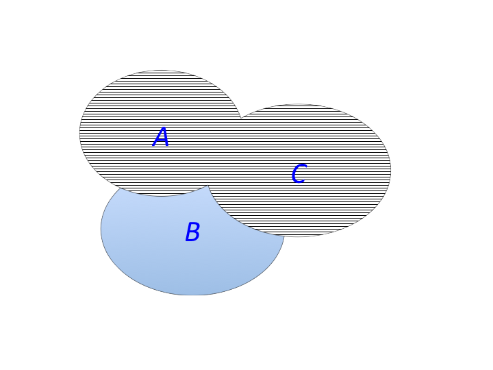
| = |  |
| ($A\cdot B) + (B\cdot C)\cdot (B+C)$ | $=$ | $(A\cdot B) + (B\cdot C)\cdot B + (B\cdot C)\cdot C$ |
| $=$ | $(A\cdot B)+(B\cdot C)+(B\cdot C)$ | |
| $=$ | $(A\cdot B)+(B\cdot C)$ | |
| $=$ | $(B\cdot A)+(B\cdot C)$ | |
| $=$ | $B\cdot (A+C)$ |
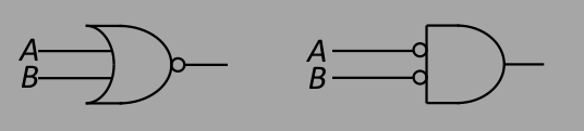
The Digital World | Back to top |
| and: $C=A\cdot B$ | or: $C=A+ B$ | xor: $C=A\oplus B$ | not: $C=\bar A$ |

| 
| 
| 
|
| $A$ | $B$ | $A\cdot B$ | $A+B$ | $A\oplus B$ | $\bar A$ | |
|---|---|---|---|---|---|---|
| 0 | 0 | 0 | 0 | 0 | 1 | |
| 0 | 1 | 0 | 1 | 1 | 1 | |
| 1 | 0 | 0 | 1 | 1 | 0 | |
| 1 | 1 | 1 | 1 | 0 | 0 |
The truth table for showing the validity of the distributive property, given for example $A\cdot (B+C)=(A\cdot B)+(A\cdot C)$ would be:
| $A$ | $B$ | $C$ | $B+C$ | $A\cdot(B+C)$ | $A\cdot B$ | $A\cdot C$ | $(A\cdot B)+(A\cdot C)$ | ||
|---|---|---|---|---|---|---|---|---|---|
| 0 | 0 | 0 | 0 | 0 | 0 | 0 | 0 | ||
| 0 | 0 | 1 | 1 | 0 | 0 | 0 | 0 | ||
| 0 | 1 | 0 | 1 | 0 | 0 | 0 | 0 | ||
| 0 | 1 | 1 | 1 | 0 | 0 | 0 | 0 | ||
| 1 | 0 | 0 | 0 | 0 | 0 | 0 | 0 | ||
| 1 | 0 | 1 | 1 | 1 | 0 | 1 | 1 | ||
| 1 | 1 | 0 | 1 | 1 | 1 | 0 | 1 | ||
| 1 | 1 | 1 | 1 | 1 | 1 | 1 | 1 |
You can see in the above truth table that the distributive property holds up.
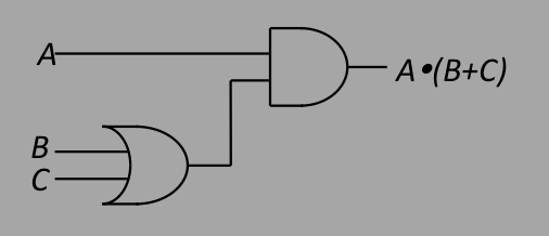
To see the utility of the distributive property, let's form the "network" of gates that implements $A\cdot (B+C)$ and $(A\cdot B)+(A\cdot C)$. First, $A\cdot (B+C)$:
Next, $(A\cdot B)+(A\cdot C)$
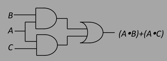
Clearly, the former might be preferred as it uses fewer gates. Back to top
Boolean Properties of Gates | Back to top |
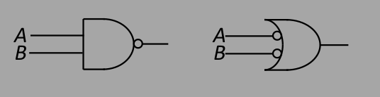
Stated in the language of logic gates, this example above says that if you take a gate and change the OR's into And's' and invert all of the inputs and outputs, you get the same logic result. This also works for the case: $$\overline{AB}=\bar A + \bar B$$ which has the following circuit equivalence:
but in plain English:
We can use DeMorgan's laws to simplify many circuits. For instance, consider the $XOR$ circuit $A\oplus B$. This circuit says "A or B but not both", which means
$A\oplus B=(A+B)\overline{AB}$
We can simplify $\overline{AB}=\bar{A}+\bar{B}$ to get
$A\oplus B=(A+B)(\bar{A}+\bar{B})$
Now we use the distributive propery and write the above as
$A\oplus B=(A+B)(\bar{A}+\bar{B})=A\bar{A}+A\bar{B}+B\bar{A}+B\bar{B}= A\bar{B}+B\bar{A}$
or $$A\oplus B=A\bar{B}+B\bar{A}$$ We can also investigate
$$\overline{A\oplus B}=\overline{A\bar B+B\bar A}= (\overline{A\bar B})(\overline{B\bar A})=(\bar A+B)(A+\bar B) =\bar{A}A+BA+\bar{A}\bar{B}+B\bar{B} =AB+\bar{A}\bar{B}\label{xorbar}$$
which means we can write $$\overline{A\oplus B}=A\oplus\bar{B}=\bar{A}\oplus B$$
Does something like $C+(A\oplus B)$ distribute to $(C+A)\oplus(C+B)$? When you work out the logic using DeMorgan's theorem, you will find that it does not.
DeMorgan's law turns out to be very useful in the world of programmable logic in that it can help a great deal in simplying logic circuits, and as you will see, when we build circuits out of the high level programmable logic language, simplification in the "compilation" can be important especially in FPGAs that have limited numbers of gates (see below). Back to top
Networks of Gates | Back to top |
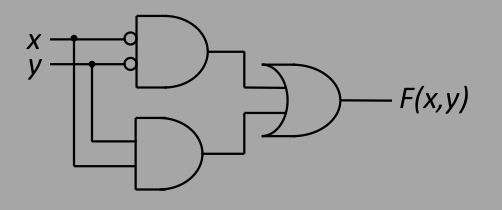
To begin, let's be slightly formal and define a 2-input function $F(x,y)$ as representing the following truth table:
| x | y | F |
|---|---|---|
| 0 | 0 | 1 |
| 0 | 1 | 0 |
| 1 | 0 | 0 |
| 1 | 1 | 1 |
$F$ is "true" (1) when $x$ and $y$ are the same (both false, 0, or both true, 1)
otherwise $F$ is "false" (0). (Let's use 0 and 1 from now on to make it simpler.)
This tells us how to construct the network: combine the terms $x$ and $y$ such that
$F$ is 1. In this example, we can see easily that $F(x,y)=\bar x\bar y + xy$.
Each "miniterm" (here $\bar x\bar y$ and $xy$) is a product ("and")
and you "sum" the products to find where the function is "true" (1), hence we call
this technique the "sum of products", or "SOP" for shorthand. The following diagram
shows the gate network that maps to $F(x,y)$:
| x | y | z | F |
|---|---|---|---|
| 0 | 0 | 0 | 0 |
| 0 | 0 | 1 | 1 |
| 0 | 1 | 0 | 1 |
| 0 | 1 | 1 | 1 |
| 1 | 0 | 0 | 0 |
| 1 | 0 | 1 | 1 |
| 1 | 1 | 0 | 0 |
| 1 | 1 | 1 | 0 |
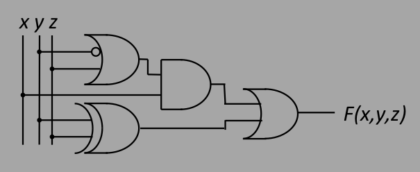
The miniterms are constructed from where $F=1$, which means the rows where $xyz=001$ ($\bar x\bar y z$), $010$ ($\bar x y \bar z$), $011$ ($\bar x yz$), and $101$ ($x\bar y z$). The SOP is therefore:
$F(x,y,z)= \bar x\bar y z + \bar x y \bar z + \bar x yz + x\bar y z$
This can be simplified by using the above rules for Boolean logic:
| $F(x,y,z)$ | $=$ | $\bar x\bar y z + \bar x y \bar z + \bar x yz + x\bar y z$ |
| $=$ | $(\bar x+x)\bar y z + (\bar z+z)\bar x y$ | |
| $=$ | $\bar y z + \bar x y$ |
where we have used the fact that $\bar x+x=1$ and $\bar z+z=1$. The gate network is
shown next:

$F(x,y)=\bar x\bar y+xy = \overline{x+y}+\overline{\bar x+\bar y} =\overline{(x+y)(\bar x+\bar y)}$
Note that we can invert $F$ and simplify to get
$\bar F(x,y)=(x+y)(\bar x+\bar y)=x\bar x+y\bar x+x\bar y+y\bar y =\bar y x+\bar x y$
Notice that $\bar xy+\bar yx$ are the two terms where $F(x,y)=0$, which is a new way to construct networks: form the product of sums where $F=0$. So we have gone from representing where $F=1$ by a sum of products to a product of sums (POS). It turns out that either SOP or POS works, and whether you one or the other may depend on details of the network. Most people think that the rule of thumb is to use the one with the fewest "miniterms": use SOP if the number of terms where $F=1$ is less than where $F=0$, or use POS if the other way around. And of course, always simplify afterwards! The following is an example of where a POS works well:
| x | y | z | F |
|---|---|---|---|
| 0 | 0 | 0 | 1 |
| 0 | 0 | 1 | 0 |
| 0 | 1 | 0 | 1 |
| 0 | 1 | 1 | 1 |
| 1 | 0 | 0 | 0 |
| 1 | 0 | 1 | 1 |
| 1 | 1 | 0 | 1 |
| 1 | 1 | 1 | 0 |
We can write down $F(x,y,z)$ using the product of sums (POS, $F=0$) and simplify:
| $F(x,y,z)$ | $=$ | $(\bar x+\bar y+z)(x+\bar y+\bar z) (x+y+z)$ |
| $=$ | $(\bar x+\bar y+z)[xx+xy+xz+\bar yx+\bar yy+\bar yz+\bar zx+ \bar zy+\bar zz]$ | |
| $=$ | $(\bar x+\bar y+z)[x+xy+xz+\bar yx+\bar yz+\bar zx+\bar zy]$ | |
| $=$ | $(\bar x+\bar y+z)[x+x(y+\bar y)+x(z+\bar z)+\bar yz+\bar zy]$ | |
| $=$ | $(\bar x+\bar y+z)[x+\bar yz+\bar zy]$ | |
| $=$ | $\bar xx+\bar x(y\oplus z)+\bar yx+\bar y\bar yz+\bar y\bar zy+ zx+z\bar yz+z\bar zy$ | |
| $=$ | $\bar x(y\oplus z)+x(\bar y+z)+(y\oplus z)$ | |
| $=$ | $x(\bar y+z)+(y\oplus z)$ |
with the following network of gates:
There are various other methods that people have employed in the past for going from a truth table to a network of gates. For instance, Karnough maps is another method of going from truth tables to gates (see the article in Wikipedia. It does not add enough to warrant more here, but suffice it to say that all of these techniques will be useful by the software that eventually builds the code that runs in programmable logic devices such as FPGAs. Back to top
Binary, Octal, Decimal, Hexadecimal | Back to top |
To set the context, a regular every-day decimal number is written in base 10, and the digits tell you how many of that power of 10. For instance, the number $3282_{10} = 2\times 10^0 + 8\times 10^1 + 2\times 10^2 + 3\times 10^3$. To convert to base 2, we will need to know how to represent $3282_{10}$ in terms of the amount of $2^0$, $2^1$, $2^2$, and so on. So it is worth memorizing (don't worry about it, if you use enough programmable logic you will end up remembering this by heart) the various powers of 2:
| $n$ | $2^n$ | |
|---|---|---|
| $0$ | 1 | |
| $1$ | 2 | |
| $2$ | 4 | |
| $3$ | 8 | |
| $4$ | 16 | |
| $5$ | 32 | |
| $6$ | 64 | |
| $7$ | 128 | |
| $8$ | 256 | |
| $9$ | 512 | |
| $10$ | 1024 | |
| $11$ | 2048 | |
| $12$ | 4096 | |
| $16$ | 65536 |
This is kind of klunky, but a computer algorithm can do this easily. Here's the trick: the using the least significant bit (LSB) of the resulting binary number will be determined by whether the decimal number to convert is odd or even. So if you divide it by $2$, then the remainder will be the LSB of the target binary number. Then you take the result of $3282/2$, and whether that is odd or even will determine the next bit of the target binary number, and so on. So the following outlines the calculation using division and remainder:
| $3282/2$ | = | $1641$ | remainder | $0$ |
| $1641/2$ | = | $820$ | remainder | $1$ |
| $820/2$ | = | $410$ | remainder | $0$ |
| $410/2$ | = | $205$ | remainder | $0$ |
| $205/2$ | = | $102$ | remainder | $1$ |
| $102/2$ | = | $51$ | remainder | $0$ |
| $51/2$ | = | $25$ | remainder | $1$ |
| $25/2$ | = | $23$ | remainder | $1$ |
| $12/2$ | = | $6$ | remainder | $0$ |
| $6/2$ | = | $3$ | remainder | $1$ |
| $3/2$ | = | $1$ | remainder | $1$ |
| $1/2$ | = | $0$ | remainder | $1$ |
Then you read off the binary number with the most significant bit (MSB) from the bottom of the above stack, and the LSB at the top: $3282_{10}=111011010010_2$.
Octal representations are in base 8, which means you only need 8 digits: $0-7$. The largest digit will be a 7, and that can be represented by the binary number $111$ since $7=4+2+1$ and the 3 digits tell us how many $4$, $2$, and $1$'s are in the number. Similarly, $6=110$, $5=101$, $4=100$, $3=011$, $2=010$, and $1=001$. Since 8 is a power of 2, there's a nice trick on how to go between binary and octal. For instance, let's take $110011010010_2$ and convert to octal by grouping 3 successive bits in a row like this: $110,011,010,010_2$. We can then read off the octal representation of the sets of 3: $110=6$, $011=3$, and $010=2$, so we get $110,011,010,010_2=6322_8$.
Hexadecimal is just as easy. Base 16 means we will need 16 digits, so traditionally we use $0-9,A,B,C,D,E,F$. The following table shows the hexadecimal, decimal, and binary representation for the digits:
| Hex Digit | Decimal | Binary |
|---|---|---|
| 0 | 0 | 0000 |
| 1 | 1 | 0001 |
| 2 | 2 | 0010 |
| 3 | 3 | 0011 |
| 4 | 4 | 0100 |
| 5 | 5 | 0101 |
| 6 | 6 | 0110 |
| 7 | 7 | 0111 |
| 8 | 8 | 1000 |
| 9 | 9 | 1001 |
| A | 10 | 1010 |
| B | 11 | 1011 |
| C | 12 | 1100 |
| D | 13 | 1101 |
| E | 14 | 1110 |
| F | 15 | 1111 |
To convert a binary number to hexadecimal, we use the same prescription as for octal but group in units of 4 and read off. For instance, $110011010010_2$ is written as $1100,1101,0010_2$, so the hex representation will be given by $CD2_{16}$. Back to top
Integers in Binary Form | Back to top |
However, this assumes all positive integers. What about negative numbers? One possibility would be to use the MSB for the sign, and the rest of the bits for the magnitude, and below there are several ways to do this. This will of course limit the largest absolute value we can represent, however there's no getting around it, we need to someone convey the sign information.
The simplest way is to just assign the MSB to the sign and use the remaining $n-1$ bits to magnitude. For example, the binary number $1000,0001=81_{16}=129_{10}$ as an unsigned number. If you assign the MSB to the sign, then this becomes $-1_{10}$. A small problem, however, occurs when considering that $1000,0000$ and $0000,0000$ seem to represent the same integer (since $-0=0$). This is not such a big deal but it's ugly and wastes precision (slightly). It is also difficult for machines to deal with (more below).
Another possibility is to use what is called the "1's complement" method. Here we complement (invert) the botton $n-1$ bits when the MSB=1. So to construct the 8-bit binary number for $-1$, you start with the bottom $7$ bits for 1, $000,0001$, complement it to $111,1110$ and add the MSB=1 to get $1111,1110$. This turns out to be better as far as integer arithmetic by machines go, however it still wastes precision since we still have the problem that $1111,1111$ and $0000,0000$ both represent $0=-0$.
A third possibility is called "2's complement". This is the same as the "1's complement" but you add a 1 at the end. So for instance, the 8-bit number $-1$ is constructed by taking the 1's complement of the 7-bit number 1 ($111,1110$), adding 1 ($111,1111$, and setting the MSB (8th bit) to get $1111,1111$. To go from binary to hex, if the MSB is set you subtract 1 and take the 1's complement. For instance, $1011,0101$ is a negative 7-bit number $011,0101$ which is the 1's complement of $100,1010$ which is $4A_{16}=74_{10}$, so $1011,0101=-74_{10}$. In this method, $0$ has a single representation ($0000,0000$), and machines can take advantage of the fact that addition and subtraction works the same on 1's complement numbers.
The following table summarizes the various techniques for a 4-bit number.
| Hex | Binary | MSB | 1's | 2's |
|---|---|---|---|---|
| $0$ | $0000$ | $0$ | $0$ | $0$ |
| $1$ | $0001$ | $1$ | $1$ | $1$ |
| $2$ | $0010$ | $2$ | $2$ | $2$ |
| $3$ | $0011$ | $3$ | $3$ | $3$ |
| $4$ | $0100$ | $4$ | $4$ | $4$ |
| $5$ | $0101$ | $5$ | $5$ | $5$ |
| $6$ | $0110$ | $6$ | $6$ | $6$ |
| $7$ | $0111$ | $7$ | $7$ | $7$ |
| $8$ | $1000$ | $-0$ | $-7$ | $-8$ |
| $9$ | $1001$ | $-1$ | $-6$ | $-7$ |
| $A$ | $1010$ | $-2$ | $-5$ | $-6$ |
| $B$ | $1011$ | $-3$ | $-4$ | $-5$ |
| $C$ | $1100$ | $-4$ | $-3$ | $-4$ |
| $D$ | $1101$ | $-5$ | $-2$ | $-3$ |
| $E$ | $1110$ | $-6$ | $-1$ | $-2$ |
| $F$ | $1111$ | $-7$ | $-0$ | $-1$ |
Computer Arithmetic | Back to top |
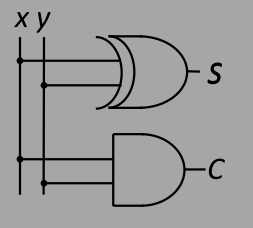
Let $x$ and $y$ be 1-bit numbers, and add them to form $S=x+y$. Best to look at the truth table:
| $x$ | $y$ | $S$ |
|---|---|---|
| 0 | 0 | 0 |
| 0 | 1 | 1 |
| 1 | 0 | 1 |
| 1 | 1 | 2 |
| $x$ | $y$ | $S$ | $C$ |
|---|---|---|---|
| 0 | 0 | 0 | 0 |
| 0 | 1 | 1 | 0 |
| 1 | 0 | 1 | 0 |
| 1 | 1 | 0 | 1 |
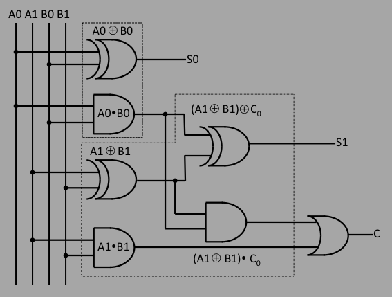
The above truth table describes a "1-bit adder". The SOP yields the equations $S=\bar xy + x\bar y = x\oplus y$ and $C=xy$. The gate network is shown below.
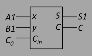
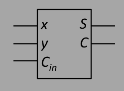
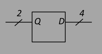
When building complicated circuits, we often take things like 1-bit adders and draw them as "black box circuits". This is in the same spirit as drawing the figure of the $AND$ gate instead of the transistors that make up the gate. For the 1-bit adder, the "primitive" might look something like this:
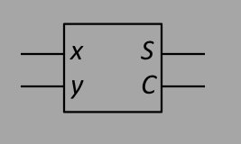
Note that each of the inputs $x$ and $y$ are 1 bit (1 line) and each of the outputs $S$ and $C$ are also 1 bit (1 line). This will change when we draw primitives of more complex circuits.
| $S1$ | $=$ | $\bar xy\bar C_{in} + x\bar y\bar C_{in} + \bar x\bar y C_{in} +xyC_{in}$ |
| $=$ | $(\bar xy + x\bar y)\bar C_{in} + (\bar x\bar y +xy)C_{in}$ | |
| $=$ | $(x\oplus y)\bar C_{in} + \overline{(x\oplus y)}C_{in}$ | |
| $=$ | $(x\oplus y)\oplus C_{in}$ |
where we have used equation ($\ref{xorbar}$) above.
Next, form the SOP for $C$ to get:
| $C$ | $=$ | $xy\bar C_{in} + \bar xyC_{in} + x\bar y C_{in} +xyC_{in}$ |
| $=$ | $xy(\bar C_{in}+C_{in}) + (x\bar y+\bar xy)C_{in}$ | |
| $=$ | $xy + (x\oplus y)C_{in}$ |
The gate network is shown directly below.

Note the dotted boxes in the figure above group $XOR$ and $AND$ gates that are equivalent to 1-bit adders. This shows the power of constructing "primitives" such as 1-bit adders to be hooked up to form 2-bit adders, as depicted in the figure below:
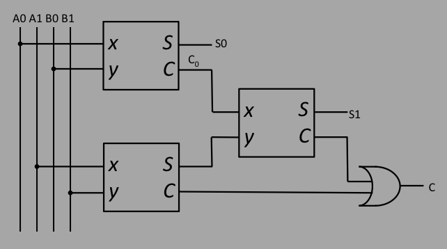
One thing to keep in mind here: because $C_0$ has to propagate through the 1st adder to get to the last one, we call this kind of circuit a "sequential adder". This means that when constructing such things, we have to keep in mind the time to propagate through real gates. While this can be fast (much less than a $ns$ in a modern FPGA), when constructing larger adders ($n-$bit adders where $n=16$ or even $32$) then there could be significan delays, and whether the delay is too large of course depends on the requirementes of the design.
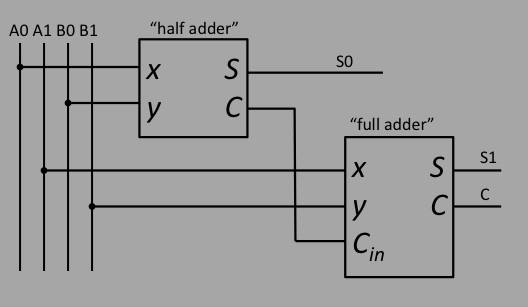
Another way to group elements in the 2-bit adder schematic is shown in the next figure:
The smaller dotted box contains the regular 1-bit adder with 2 inputs, sometimes also called a "half adder":

and the larger box contains the 1-bit adder with the 3 inputs, aka "full adder":
We can put these 2 together to construct a 2-bit adder as shown below:
As you might expect, we can extend the pattern for the 2-bit adder to make an adder with any number of bits in analogy to how we can extend the algorithm for adding the 2-digit numbers together to any number of digits: add digits, save the carry bits, use it to add to the next highest bits until done. The following diagram illustrates how this is done for a 4-bit adder (adding 2 4-bit busses: $S[3:0]=A[3:0]+B[3:0]$. Note that we've redrawn the half and full adders to make the diagram more "linear", with the carry output of 1 adder flowing to the right into the $C_{in}$ input of the next one. This is sometimes called a "ripple adder", since the carry bit ripples through. As such, this is also a sequential adder that has a timing determined by the time through all the adders.
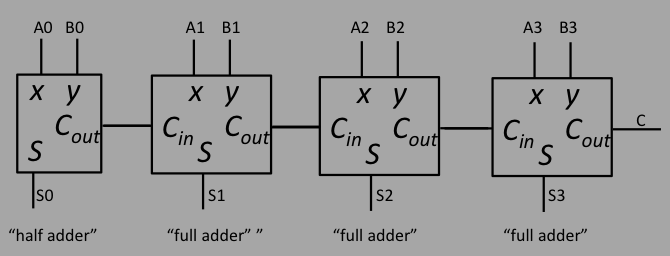
There are of course ways to build $n$-bit adders that are not sequential, and therefore faster. This will not be covered here, other than to say that in the world of digital logic and gates, there is a "phase space" that consists of number of gates $N$ vs total time through a circuit $T$, and that often it is the case that $NT=constant$. That is, one can make a circuit "faster" (smaller propagation time) but it will cost you gates. Or one can make a circuit "smaller" (fewer gates) but it will be more sequential and thust be "slower" (larger propagation time). Back to top
Useful Primitives | Back to top |
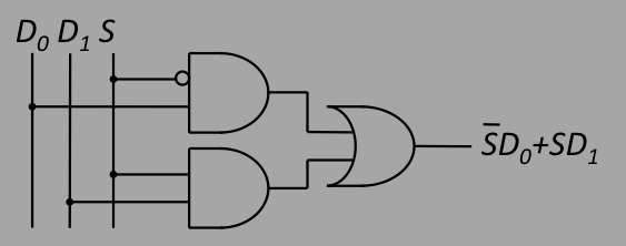
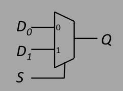
A "mux" is a circuit that takes 2 inputs, and depending on the state of a selector, connects one of the inputs to the output. A mux with 2 1-bit inputs, $D_0$ and $D_1$, will connect one of them to the output $Q$ depending on the state of the selector $S$. To be specific, when the selector $S=0$, then the output $Q$ is given by $Q=D_0$. When $S=1$, $Q=D_1$. This is called a "2-1 mux". The truth table would yield the equation $Q=\bar S D_0 + SD_1$ and the gate network looks like this:
The primitive looks like this for a 1-bit input and a 1-bit selector:
If we want to extend this to a mux with 2-bit inputs ($A[1:0]$ and $B[1:0]$), then since there are 2 inputs we still need a single selector (a selector that is 1 bit wide), so we would just use a pair of 2-1 muxes, one for $A0,B0$ and one for $A1,B1$.
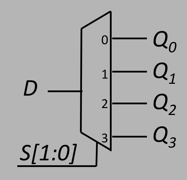
One can also imagine a mux that will connect one of 4 (or more) inputs to the output, The inputs will be $D_0$, $D_1$, $D_2$, and $D_3$, and the output will still be a single bit $Q$. Since we now have to choose between 4 inputs, we need a selector that is 2-bits wide: $S[1:0]$. This is a "4-1 mux", with the following truth table on the selector:
| $S_0$ | $S_1$ | $Q$ |
|---|---|---|
| 0 | 0 | $D_0$ |
| 0 | 1 | $D_1$ |
| 1 | 0 | $D_2$ |
| 1 | 1 | $D_3$ |
This gives us the following equation for the output: $Q=\bar{S_0}\bar{S_1}D_0 +\bar{S_0}S_1D_1 + S_0\bar{S_1}D_2 + S_0S_1D_3$ and the following for the 4-1 primitive:

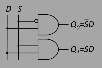
A "demux" is the opposite of the "mux": sending an input to an output depending on a select. The primitive looks like this:
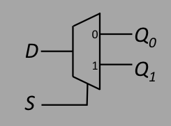
What we want is a gate network that will send $D$ into $Q_0$ when $S=0$ and $Q_1$ when $S=1$, which means $Q_0=\bar{S}D$ and $Q_1=SD$. The corresponding network is:
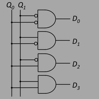
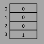
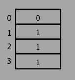
A decoder circuit will take a binary number and decode it to show which
bits are asserted. For instance, if you have a 2-bit number $Q[1:0]$,
the 4 possible numbers it could represent are $0,1,2,3$. A decoder will
have 4 outputs, say $D_0,D_1,D_2,D_3$, and will assert each of these
according to the value for $Q$. For example, if $Q=1$, then the decoder will assert
$D_1$ and deassert all the others.
The truth table, gate network, and primitive are below:
Interestingly, there's a correspondence between the 2-bit decoder and a 1-4 demux.
The latter looks like this:
A comparitor can be used to test the value of a number represented in gates. To make
things easy, let's construct a 1-bit comparitor using two signals, $A$ and $B$, and
forms 4 outline lines that are high ("asserted") when $A\!=\!B$,
$A\!\lt\!B$, $A\!\gt\!B$, and
$A\!\ne\!B$. The truth table for this is:
You should be able to recognize that the last column, $A\!\ne\!B$, is clearly an
exclusive or: $A\!\oplus\!B$. Similarly, the 1st
column, $A\!=\!B$, is clearly the inverse of $A\!\oplus\!B$. Using SOP it is
easy to see that the gates for
$A\!\lt\!B$ is $\bar A B$ and $A\!\gt\!B$ is $A\bar B$.
Back to top
Decoder
Truth Table Network Primitive
$Q_0$ $Q_1$ $D_0$ $D_1$
$D_2$ $D_3$
0 0 1 0 0
0
0 1 0 1 0
0
1 0 0 0 1
0
1 1 0 0 0
1

Comparitor
$A$ $B$ $A\!=\!B$ $A\!\lt\!B$
$A\!\gt\!B$ $A\ne B$
0 0 1 0
0 0
0 1 0 1 0
1
1 0 0 0 1
1
1 1 1 0 0
0
Memory (Registers) | Back to top |
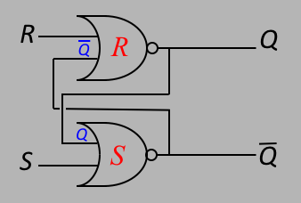
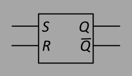
Imagine we construct the following gates to connect inputs $S$ and $R$ to outputs
$Q$ and $\bar Q$:
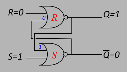
Now specify the input values: $R=0$ and $S=1$.
The inputs and outputs are shown below,
and the blue just follows the outputs.
You can see that since the bottom gate $S$ has
both inputs set ($S$ and $Q$
are both $1$), then if $S$ deasserts, $Q$ and $\bar Q$ remains the same, inverses of
each other. That's why we call this a "latch", because it latches the value
of $S$, and due to feedback, "remembers" it.
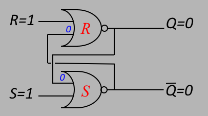
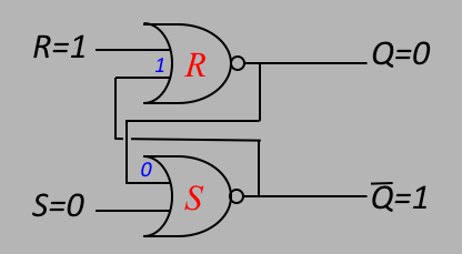
Now let's consider what happens when you are in the "set" state, $S\bar R$, and you
switch from $S=1$, $R=0$ to $S=0$, $R=1$. Let's analyze this by first asserting
$R=1$, seeing how the latch responds, then deassert $S=0$ and check again.
Setting $R=1$:
If instead of driving $R=1$ (and then $S=0$) you first drove $S=0$ (and then
drove $R=1$), giving $R=S=0$ as the intermediate state, nothing would
change due to the feedback.
The above combination is called a $SR$ "latch", or more precisely,
an $SR NOR$ latch. The "latch" means that the gadget "latches" the incoming
"set" and "reset" signals.
The function table, like a truth table, can be constructed like this:
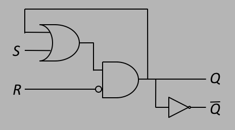
We can make an even simpler and more well behaved version of the RS latch
by constructing it from a single AND-OR gate combination, as in the figure
below:
When you set $S=1$, this turns on the OR gate (no matter what the other input
is doing), and if you set $R=0$, the AND gate turns on, setting
$Q=1$: the system is "set".
If you then turn $S$ off, nothing happens, the system "holds". If you
turn on $R$ ($R=1$), then that turns off the AND gate no matter what
$S$ is doing, driving $Q=0$. SO the truth table here is equivalent,
but simpler than the one above:
The "X" above means "don't care". $R$ is a true "reset", and once the
gate enteres the "set" state, it will stay there ("remembering") until
you drive $R=1$ to reset it.
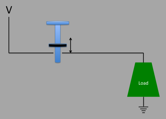
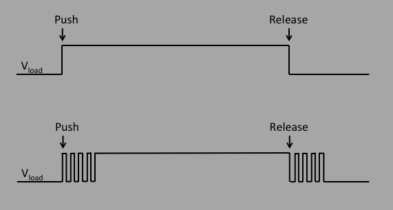
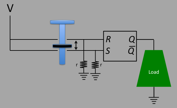
An example of where an RS latch can be very useful is as a "debouncer". So imagine
that you have a mechanical button, and when pushed it connects some output to a voltage
source as in the figure below.
Note that this debouncer is sending a digital signal to the load, so this
would technically be called a "digital debouncer". (That is, we are not
considering analog debouncers!)
Sometimes you might want restrict the period time in which an RS latch is
active (that is, will respond to changes in $R$ and $S$). In other words,
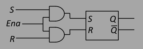
you want to set up an "enable". This is accomplished by adding AND gates
to the inputs. The following shows the network needed to add the enable
ENA, and the resulting primitive:
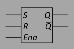
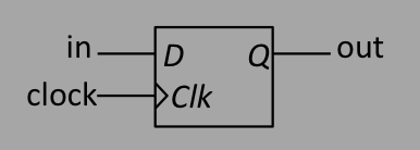
A "D-latch" ("D" for "data") is an RS latch where we take care of the $R$ and
$S$ being inverses of each other, and just use a data line $D$, with an enable.
The latch, when enabled, will have an output $Q$ that follows the data input
$D$:
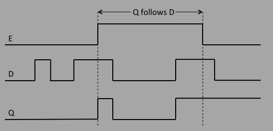
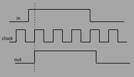
The waveform will look like this:
The output $Q$ will "follow" the input "D" only when $E$ (the enable) is
asserted.
As seen above, the gated D-latch has an output that follows the input as long
as $E$ is asserted. But sometimes you just want to have the output follow
the input at a single specified time and not a range of times. For instance,
you might want to have a signal that transitions from 0 to 1, and at that time
of transition, you might want to have the latching happen. The diagram that
describes this is similar to the one above, except that the latch only happens
at the "positive edge" of the enable $E$, and anything later is ignored. This is
called an "edge triggered flip-flop", or DFF for short:
In the above primitive, instead of labeling the edge signal with "ENA", we label it
with "Clk", or "clock".
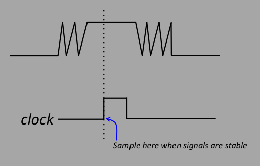
This brings up an important concept that is worth emphasizing: with edge triggered
DFF's, we now can implement what is called "synchronous logic", as opposed to the
previous implementions of what is called "combinatorial logic". In synchronous logic,
everything happens synchronously, or in sync with, some signal. And it is natural
to consider synchronicity in the context of some kind of "clock" that keep things
synchronous.
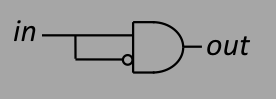
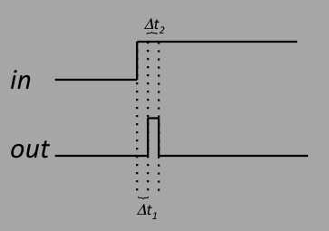
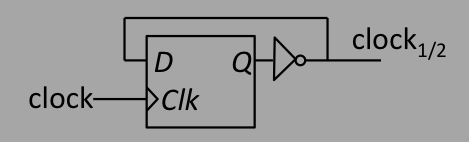
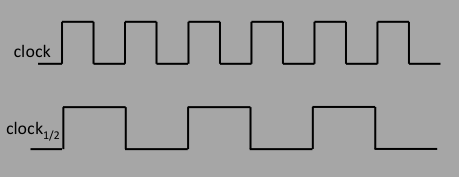
It turns out to be quite simple to make an edge detector. We start with the
circuit and waveform below:
RS (NOR) Latch
"Set" State
"Reset" State
This gives an output that has $Q=\bar Q=0$, breaking the symmetry that $Q$ and
$\bar Q$ are inverses of each other.
The figure below shows this intermediate state:
So the result, as shown in the figure below, has $Q=0$ and $\bar Q=1$, $Q=0$,
and again $Q$ and $\bar Q$ are inverses of each other. This is called the "reset"
state.
$S$ $R$ $Q$ $\bar Q$
function
1 0 1 0 set
0 1 0 1 reset
0 0 $Q$ $\bar Q$
hold
1 1 0 0
$Q\ne\bar Q$
RS (AND-OR) Latch
$S$ $R$ $Q$ $\bar Q$
function
1 0 1 0 set
X 1 0 1 reset
0 0 $Q$ $\bar Q$
hold
Debouncer
Gated RS Latch
Gated D Latch


D Flip-Flop (DFF)
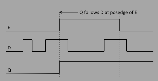
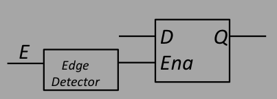

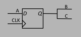
Figure 1, the D-flip flop.
Synchronous Logic | Back to top |
| 
|
| 
|
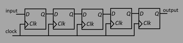
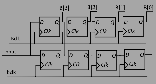
What could this be used for? One example is in serial to parallel data transmission. Imagine you are sending a serial 4-bit signal, and you want to decode it to know what the 4 bits are. These 4 bits will come in 1 by 1, at some rate synchronous with a "bit clock" ($bclk$). You place them into a 4 DFF long shift register, form a "byte clock" ($Bclk$) that is $1/4$ the "bit clock", hook it and latch the byte into a 4-bit wide "byte register as in the figure below. We are assuming that the bits arrive such that bit 0 comes first, followed by bit 1, 2, and 3, and repeats. The nomenclature is such that $B[3]$ is the 4th bit (MSB for "most significant bit"), and $B[0]$ is the 1st bit (LSB, for "least significant bit").
(Finite) State Machines (FSM) | Back to top |
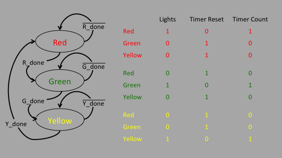
The classic example is a traffic light control. Here we have 3 states: red ($R$), green ($G$), and yellow ($Y$). The machine will step through these states in a definite order ($R\to G\to Y$), and will turn on and off the red, green, and yellow traffic lights.
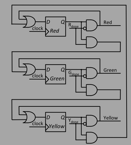
It is often helpful to diagram the FSM to help visualize what happens when. Our traffic controller FSM would look like this. The "Red", "Green", and "Yellow" table enters are color coded to represent their values in each of the 3 different states.
Pretty simple and straight forward, but how do we construct such a thing? We start by using DFFs to store the state, and a build a logic network for the transitions and controls.
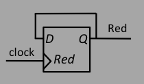
Let's start in the red state. We use a DFF with a preset of 1 (preset to be on) with feedback to "hold". The circuit looks like this:
When the red timer Now we have to add the transition to the green state, which happens when the state is $R_{done}$ goes off, the state should transition, so it is no longer in the red state. That means you have to turn the red DFF off. The circuit to accomplish this would look like this:
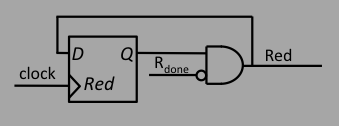
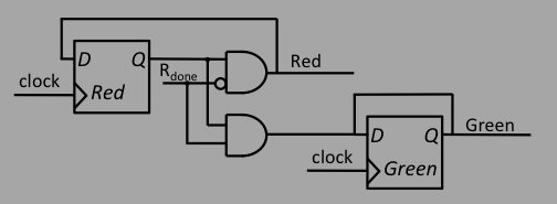
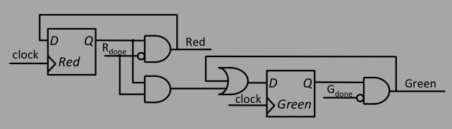
Keep in mind that there will be propgation delays through the dates, so care should be taken to make sure that we don't inadvertently turn on two lights at the same time! And that one should try to have the clock inputs in such a way that the positive edges of each clock occur at the same time. This is easy to do, however, since the traffic FSM will not need $\mu$sec precision, so all you have to do is use a "fast" clock, which implies counters that are large to count macroscopic times.
A timing diagram is a very good complementary way to help describe how you want a state machine to behave. For our machine, we show the clock, the inputs from the red, green, and yellow timers ($R_{done}$, $G_{done}$, $Y_{done}$), and the outputs that turn on the lights, timers, and reset the timers ($Red$, $Green$, and $Yellow$).

Note that the $R_{done}$ pulse is generated from the condition that the red counter is
finished (as a countdown counter, it's the condition that all bits are 0). But once
that condition is met, $R_{done}$ should stay high as long as the counter is at 0.
What is shown, however, is a pulse. This is a common thing to do to control things
carefully: we make $R_{done}$ a pulse so that we don't have any problems with illegal
states and illegal transitions. This "just in case" technique is a matter of taste,
however it is always wise to never leave active signals in the active state even
though you think nothing is paying attention to it! How we change $R_{done}$ from a
level to a pulse is easy: we implement something called a "one-shot".
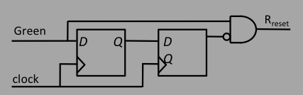
One Shot
The diagram below shows how to build a "one-shot", a circuit that changes a level into
a pulse. As pertains to the traffic system, when the green state is entered, GREEN
is asserted, and we want the red timer to be reset (reset to its preset value, and
ready and waiting to start counting). Before GREEN is asserted, the lower part of
the AND gate is asserted. Once GREEN goes high, then the gate turns out, and the
output $R_{reset}$ follows GREEN. Once the GREEN signal gets through the 2 DFFs, the
AND gate turns off and so does $R_{reset}$, turning the GREEN level into a $R_{reset}$
pulse. Once the red counter is reset, $R_{done}$ will also no longer be asserted,
and it will transition to 0 (as in the diagram).
Programmable Logic | Back to top |

Necessity is the mother of invention. Take a look at the following truth table that implements and AND gate:
| x | y | xy |
|---|---|---|
| 0 | 0 | 0 |
| 0 | 1 | 0 |
| 1 | 0 | 0 |
| 1 | 1 | 1 |

Modern FPGAs can contain the resources for making the equivalent of millions of gates, allowing all sorts of things to be implemented, even small 8-bit CPUs. They also have dedicated RAM to be used for memory purposes called "block ram", or BRAM, with upwards of many MBytes. They can have clock managers ("digital clock managers") that allow clock cleanup, phase adjustment, and clock multipliers, and some have built-in hardware arithmetic and modest CPUs. Back to top
Download Vivado | Back to top |
Befor getting into HDL, you should first download and install the Xilinx program Vivado. For this tutorial (2017), it is recommended you get Vivado 2017.2 (or .higher). To do this, either follow this perscription:

Run the appropriate installer, and set up a license. It is ok to get the 30 day trial license, but for the longer haul you should set up a better version, and as far as I know, at this time the licenses are free.
Hardware Description Languages (HDL) | Back to top |
The task of using FPGAs consists of 2 important steps: 1) deciding on the logic you need to implement, and 2) implementing it on the specific chip. Part 1 is your job, consisting of either drawing the gate network using some kind of palette and putting things together, or writing code in some higher level "hardware description language, or HDL". HDL, an a specific implementation called "Verilog", is what will be introduced and covered in this section. Part 2 is the job of the company that makes the FPGA, and will consist of several steps: 1) synthesis of the output of part 1, your part, to figure out the list of gates and DFFs etc that you will need, and how they are connected (a "netlist") so as to implement the logic that you want, and 2) a "place and route" (PAR) that determines how and where to place the resources needed and how to route the signals from one place to the other, relative to whatever specific FPGA you are going to use to implement the deesign. This PAR step can take a lot of CPU time depending on the nature of the job, how "full" the FPGA is (fraction of resources used) and what the constraints are for meeting timing goals.
There are 2 basic HDL languages that are used, called VHDL and Verilog, and they are both born from the need to simulate designs. Verilog was developed by players in the private sector in the early 1980s for simulation, and the name comes from the synthesis of "verification" and "logic". The language itself began as a proprietary product owned by Cadence, and was put in the public domain as an IEEE standard in the mid 1990s. VHDL on the other hand was developed by the DOD for ASIC (application specific integrated circuits) production, all the way down from the logic to the hardware level. In VHDL you can specify things like transition emitter rise time, and other things that have nothing to do with the design logic. As such, VHDL has many more constructs (syntax) than does Verilog, which makes it both richer and more complex. For pure programmable logic, implemented on FPGAs, many find Verilog to be easier to use, but this is just an opinion (that of course borders on religion for some of the more focused people!). We will focus on Verilog here.
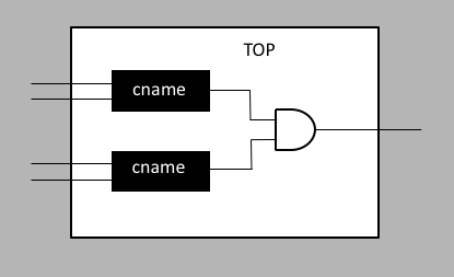
But basically, you should think of the code in terms of circuits: the code defines circuits,
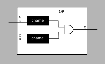
which means inputs, outputs, and what's in between. The following picture shows a top level
circuit called "TOP", with 2 inner circuits named "cname". TOP has 4 inputs (on the left) and
1 output (on the right), cname has 2 inputs in the left and 1 on the right. None of the inputs
are labeled now. The syntax is:
First lets define the inputs as A, B, C, D, and the output as O, and use the usual
Verilog syntax for defining the top level "module" which we will call "TOP".
The
syntax structure is the following:
We don't yet know what "wire" means, but that will come next.
There is no semicolon after the "endmodule", but there is after the "module" at the beginning.
"name" can be anything, and the inputs and outputs are specified inside the parentheses.
Below the "module" declaration, you specifiy which are inputs and which are outputs, and then
whether they are wires or regs (see below). Note that the above syntax is pretty much from
the original incarnation of Verilog, which is evolving, so of course there's a more compact
way of doing the above:
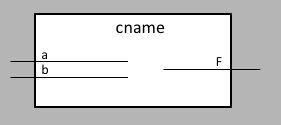
Now that you have the TOP circuit coded up, you have to also code up "cname".
We don't know what's inside of "cname", and we don't need to know that yet, but we do have to
know that it has inputs and outputs. So we label the inputs as "a", "b", and the output
as "F". The following figure shows the cname circuit:
Verilog has a nice way to get around this potential disaster of wiring the inputs
wrong from the top level module where the circuit is instantiated. For instance, you might
have wanted to instantiate it as "cname CNAME1(B,A,c1);" instead! So to get around
this potential for disaster, Verilog have an alternate way of wiring up inputs and outputs
from one circuit into another. The new way is shows below:
We specify the lines as "wires", and these are objects that can be thought of as being just like real
wires in circuits - the wire will be driven by something (like an AND gate) and will have a value
(or state) of 0 or 1. Note that wires only carry the value from the thing that drives them.
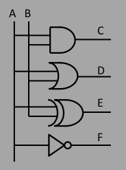
From the above figure with inputs A,B and outputs C,D,E,F, the first piece of Verilog syntax will be:
Now comes the part that contains the logic you want to implement.
In Verilog, we have the following representations of operations and
operators:
That's it! Pretty simple.
As an aside...why does Verilog have an "assign" statement and not require it? It's because
of the history of Verilog, and it's original usage, which was as a simulation language.
Imagine writing some computer code to simulate a digital network (like the one we just
invented above, with TOP and cname). You would have to have some kind of timescale "tick",
and at every tick you see what the signals are doing, and propogate things to the next time.
If your simulation consists of 4 inputs, 1 output, and a couple of internal wires, then it's
easy. But if the simulation is more complicated, then to check everything at every time tick
will be exceedingly slow.
So Verilog, originally a simulation language, solves this by inventing the "assign" statment.
Here's how it works for the statement
Now let's make a new design that uses everything we've learned, and write code that
instantiates the following circuit:
We are ready now to code up the finite state machine (FSM) that we invented for the traffic light.
For this project, we will need an externally provided clock input, and let's put the frequency
(arbitrary, but we have to pick something) at 1kHz, or 1.0ms time period.
Now, let's set the time for the lights to be (roughly, this doesn't have to be exact)
30s for green, 30s for red, and 2s for yellow. That means we need to wait $30s/0.001s=30,000$ ticks
for the green and red light, and $2/0.001=2,000$ ticks for the yellow.
This dictates that we need a 15 bit counter: $2^{15}=32768$, which means it will count for
$32.768$ seconds, which is close enough. For the yellow light we need an 11-bit counter:
$2^{11}=2048$ which means the yellow light will be on for 2.048 seconds, also close enough.
Let's make a top level module called "TRAFFIC", and have 1 clock input and 3 enables for the
3 different lights:
The timers are instantiated like this:
Now that we have the timers and the timer done lines, we can write the code that
controls those timers. Since the timers are registers, we implement it in an always
block. We need an enable line that controls when to allow the timer to count down,
and what to do when the timer is not counting (reset to all 1's). The code
for the red timer will look something like this:
Also, note that in the ILLEGAL state, we specify all of the outputs,
not just the red light. This is because if we got into ILLEGAL, we don't
really know how that could have happened (an electrical glitch?), so we
want to be sure we are controlling everything.
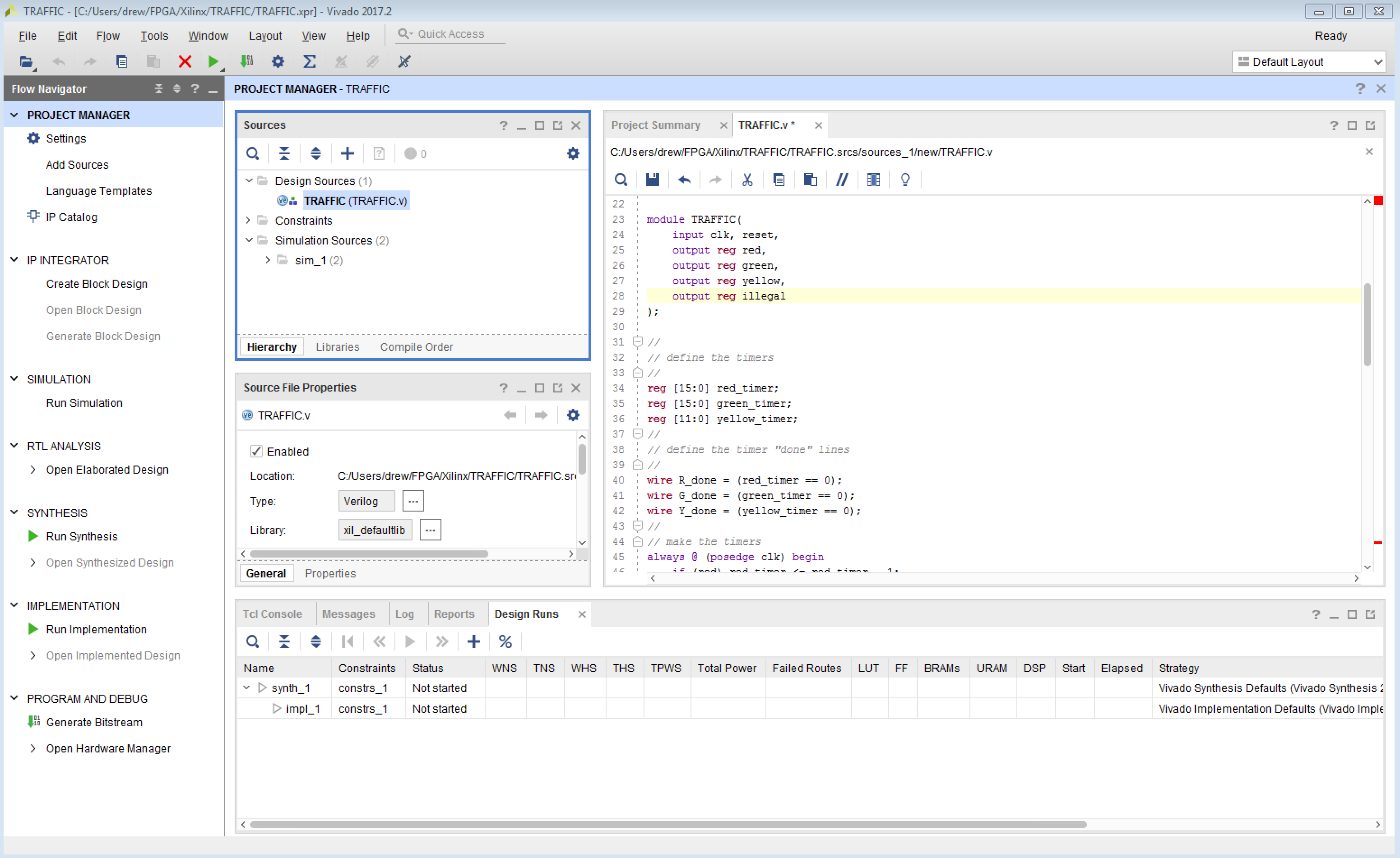
We now have to start using the Xilinx Vivado program. The version
here (2017) is v2017.2 running on a Windows machine. See
above for instructions on how to download and install. Once that is complete, and you have
a valid license installed, run Vivado "HLx" (not "HLs"!).
When you run Vivado, you should see the following screen:
The next screen is called "Project Type". Click on the 1st radio
button labeled "RTL Project", and hit "Next".
Next you will go to "Default Part". This is for people who know
the part name of the FPGA they will be programming. In this case,
we don't really care about the actual FPGA, so just it "Next"
without specifying anything. That takes you to the final window
where you can hit "Finish". You should now be at a window that looks
like this:
Now we need to add some source code. If you mouse over
the "+" sign in the "Sources" subwindow, it should say "Add Sources (Alt+S)".
Click there to bring up the "Add Sources" window. Make sure that
"Add or create design sources" is set, and hit "Next". This brings up a
window called "Add or Create Design Sources". Since you don't have any
sources, you want to click on the box called "Create File", as seen
below:
The Vivado window should now look like this:
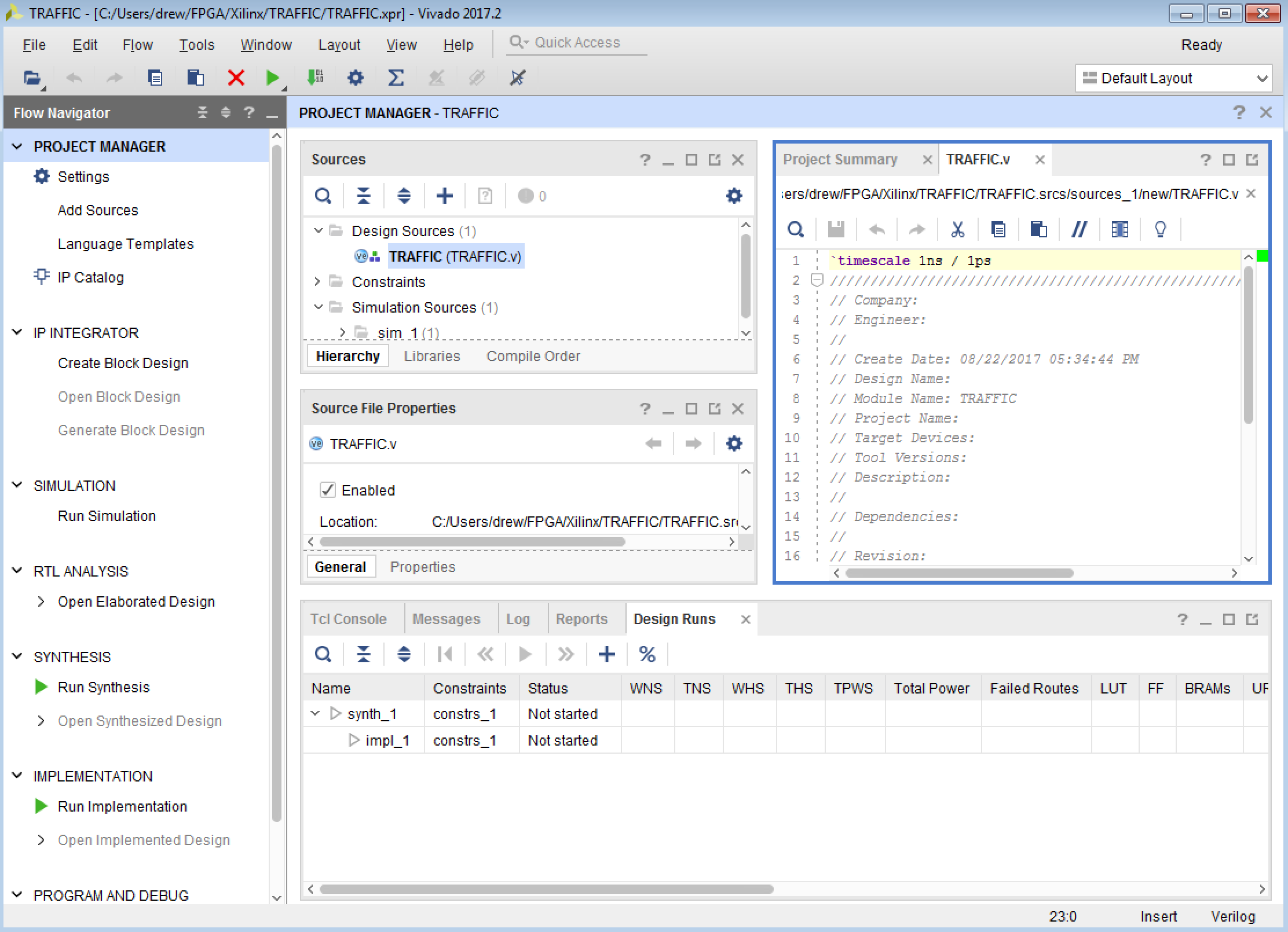
The top line of TRAFFIC.v has the following line of code:
Now go to the traffic FSM you coded up earlier, paste that into
the edit window, and save it (control-S).
It should then look like this:
Before you take any Verilog code you've written and run it in an FPGA, you
should always run a simulation and look at waveforms. This is really
important for any successful programmable logic project, because as we know
form Murphy's law, nothing ever works correctly the first time.
Let's use the FSM for the traffic lights that we wrote in the previous
chapter. We will simulate it using the standard tool that comes in the
development tool from Xilinx (or Altera, take your pick), but first we
have to write our own "stimulus". That means we need to write some
Verilog that controls the inputs to our circuit ("TRAFFIC"), and checks on
the outputs, and presents them in a viewable waveform. There are tools
that allow you to generate stimulus using waveforms directly (pointing and
clicking), however it's much more powerful to use Verilog directly, and
the bottom line is that a simulation is only as good as the ability to
faithfully represent the inputs.
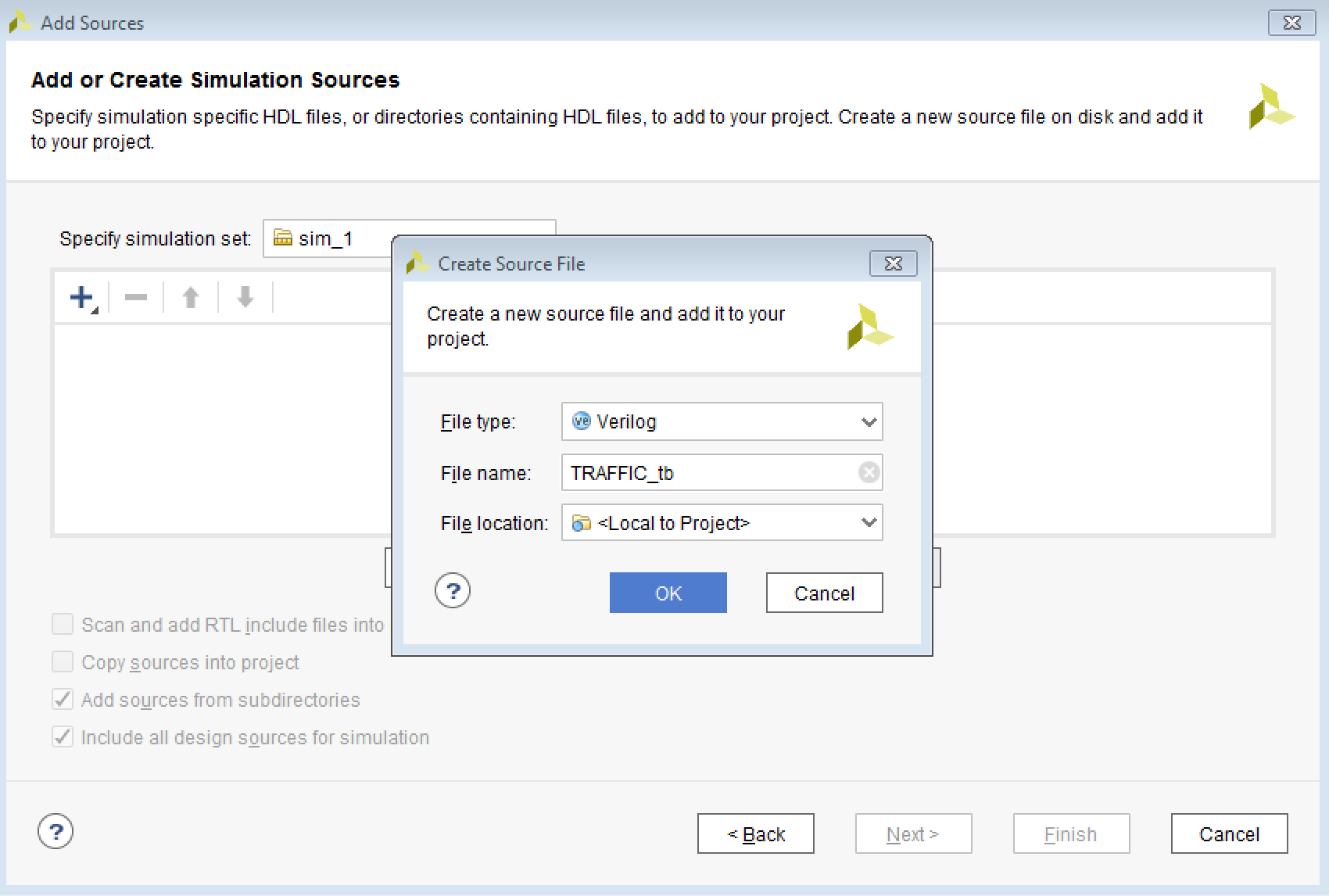
To generate the testbench, we first generate a new source file that
will be plugged into the project. In the same "Sources" subwindow
that you used create the TRAFFIC.v source, click again on the "+"
button to bring up the "Add Sources" window. This time click on the
3rd choice, "Add or create simulation sources",
and click "Next". The brings up the "Add or Create Simultion Sources"
window, where you click "Create File", which brings up a "Create Source File"
window where you can name the new source. Let's call it "TRAFFIC_tb"
("tb" for "testbench") and it OK. It should look like this before you
hit OK:
Hit OK and "Finish", and "OK" at the next "Define Module" window, and
confirm "Yes". Vivado should look like this now:
Next we have to edit TRAFFIC_tb.v to add the stimulus. To do this,
click on the ">" symbol on the line "sim_1". It should then show
you 2 files: TRAFFIC.v under "Design Sources"
and TRAFFIC_tb.v under "Simulation Sources". The latter is what will
use to stimulate the former.
If all is well you should see the correct hierarchy like in
the following, with "TRAFFIC.v" underneath "TRAFFIC_tb.v".
Double click on TRAFFIC_tb.v and it will create
a new tab in the subwindow to the right. That window should be
empty except for the timescale directive, some comments, and
the module declaration. Now we learn how to write Verilog stimulus code.
The first thing we want to do is to instantiate the TRAFFIC.v circuit,
and define the inputs that go
into TRAFFIC.v, so that we can stimulate them, and the outputs,
so we can see how they behave. We do this with the following code:
Next we want to specify the reset line, which is done in the following
code:
Now we are ready to run the simulation. In the left pane of the Vivado
window, you should see "Run Simulation". Click on it and you should see
a pop-up window. Click on the top line, "Run Behavioral Simulation".
What that means is the following: the verilog code for
TRAFFIC.v has no timing information (it's actually possible to add it,
but that's another story). So when AND and OR gates change state, and
DFFs see posedges, they happen "instantly". As such, the waveforms will show
the behavior of the logic, but won't tell you anything about actual timing.
Doing that is possible, but only after you've actually run the full
synthesis and implementation. I have found that most of the bugs are
found right away by doing a behavioral simulation. If you have timing
problems (so-called race conditions) then you probably won't see them in
any kind of simulation easily, you just have to run the thing in an FPGA
and do a first order checking there for mistakes before a real timing
simulation. Also, the timing simulation uses best guesses for the actual
delays inside the FPGA. And each FPGA is slightly different. Best to
find errors in situ first!
If you have any errors, the system will report it. On the bottom, you
will see a panel with 5 tabs labelled "Tcl Console", "Messages", "Log",
"Reports", and "Design Runs". You will have to wade through these to
figure out what the errors are, but usually it's just syntax. The
"Tcl Console" should tell you the exact errors.
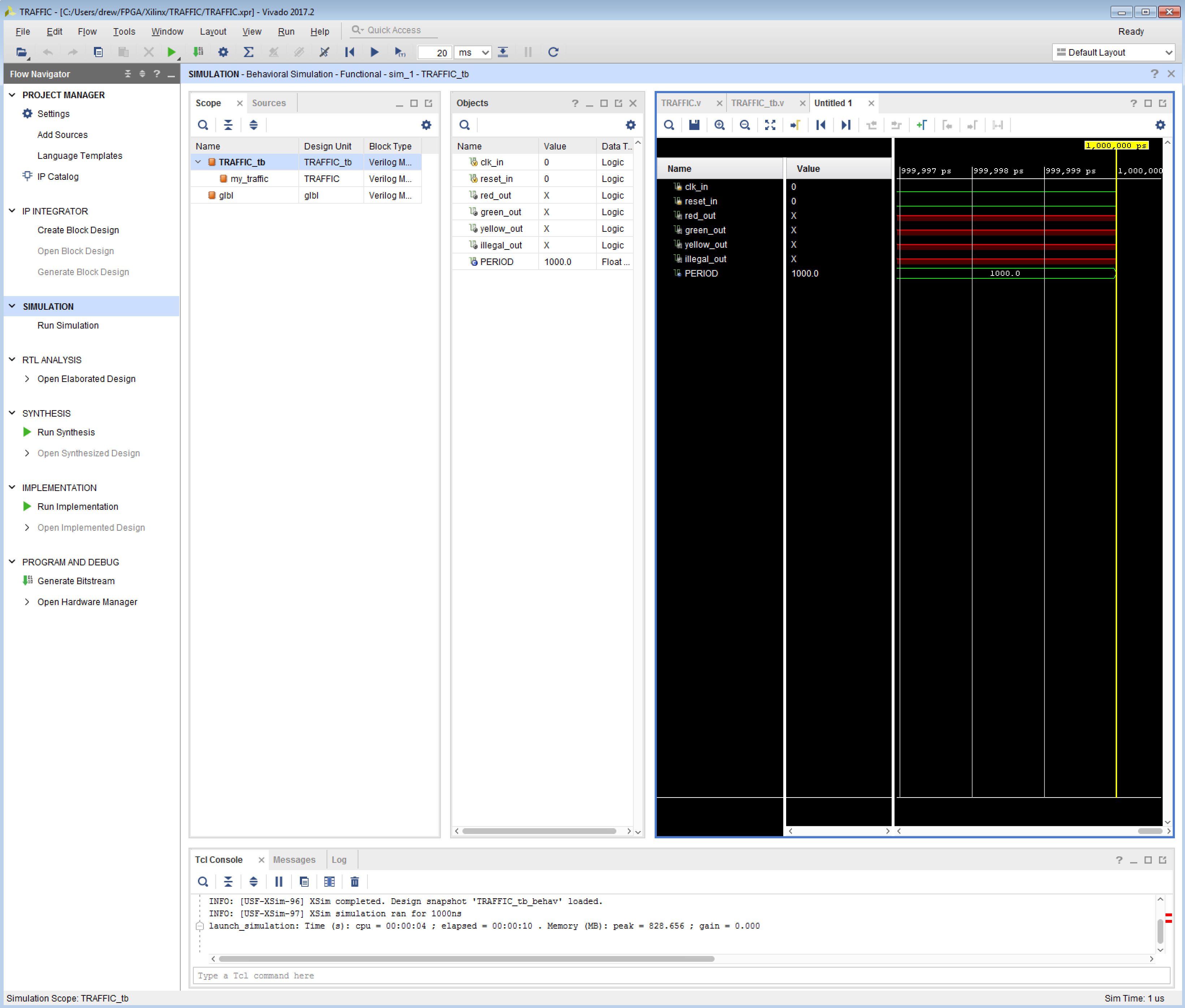
Assuming all goes well, you should now be looking at the following
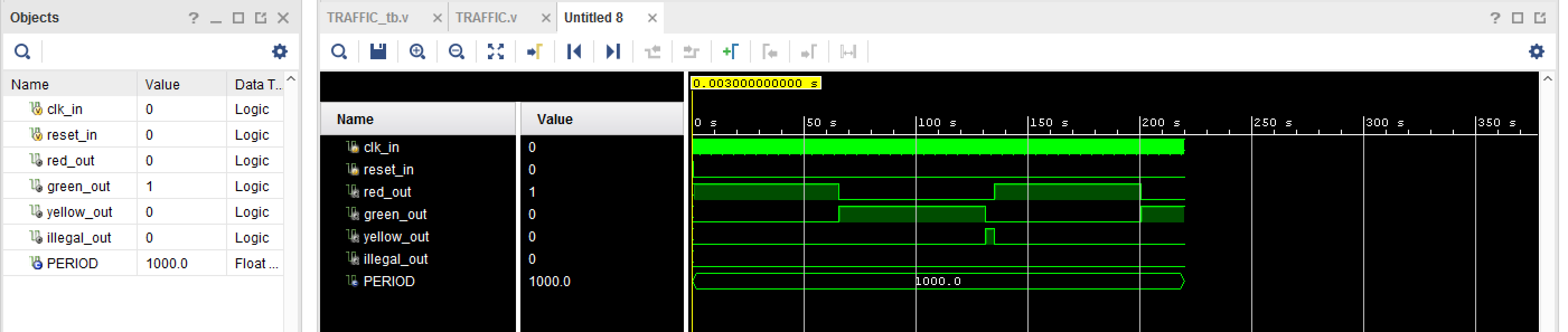
rather large window:
The default scope is "TRAFFIC_tb", so you can see in the waveform window
all of the signals present in that source. You won't see anything
interesting yet, because the simulation defaults are not set correctly.
Notice on the top line of the window the usual tabs "File", "Edit", etc.
Towards the end, you will "Quick Access". There are 3 icons, then
a text window that says "20", then one that says "ms", then some other
icons. The first of the 3 is the "Restart" icon, for restarting the
simulation. The next one, a triangle, is "Run All" (run), and the 3rd
is a triangle with a little "m" below it, which means run for a time
period as specified in the next 2 windows, which means 20ms. Let's
change the "ms" to "s", click restart, and click run for 20s.
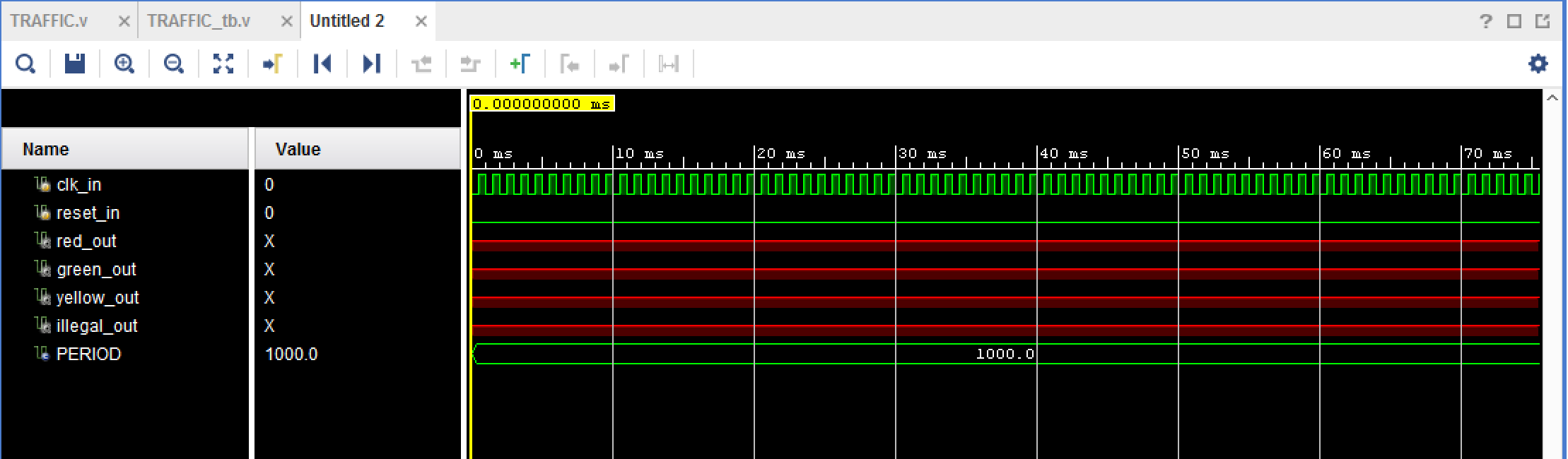
Now, go into the waveform window and click on the icon that is called
"Go to time 0" (when mousing over), and then keep zooming in (3rd icon,
circle with a + sign) until you can see the clock transitions, so the
vertical lines should be every 10ms or more. You should see something
like this in that window:
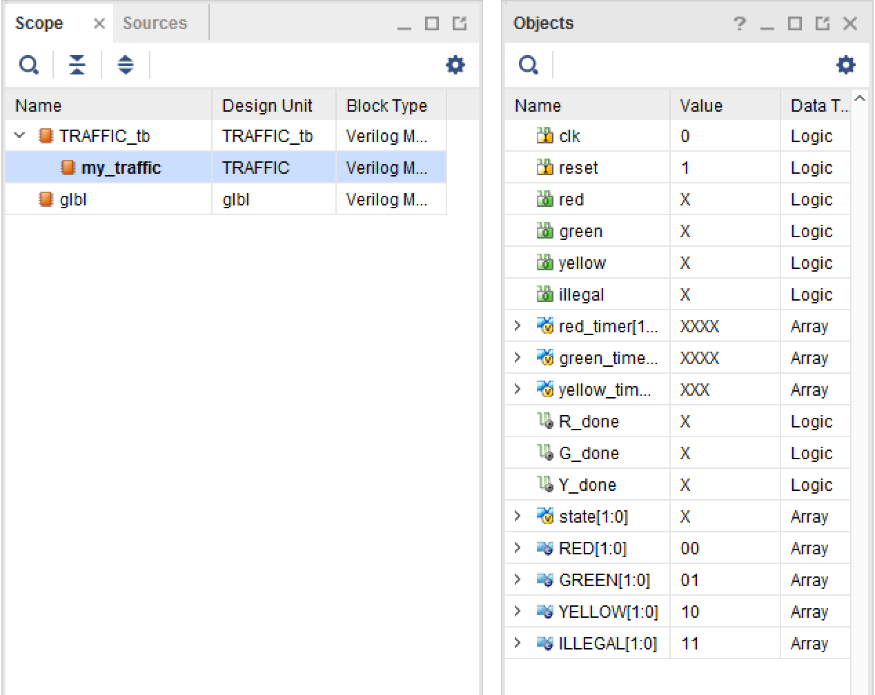
One nice technique to figure out what needs to be defined is to click
on the "my_traffic" scope in the Scope window. That will bring up all
the objects. You will see which have the value "X", as in the following
window:
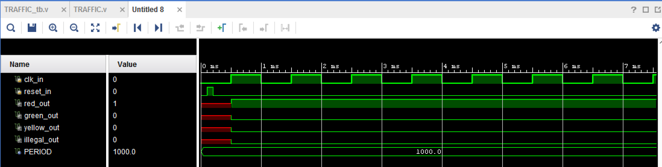
Here, we want to do an asynchronous reset, because it's only going to happen
once. The first thing to change is the stimulus code:
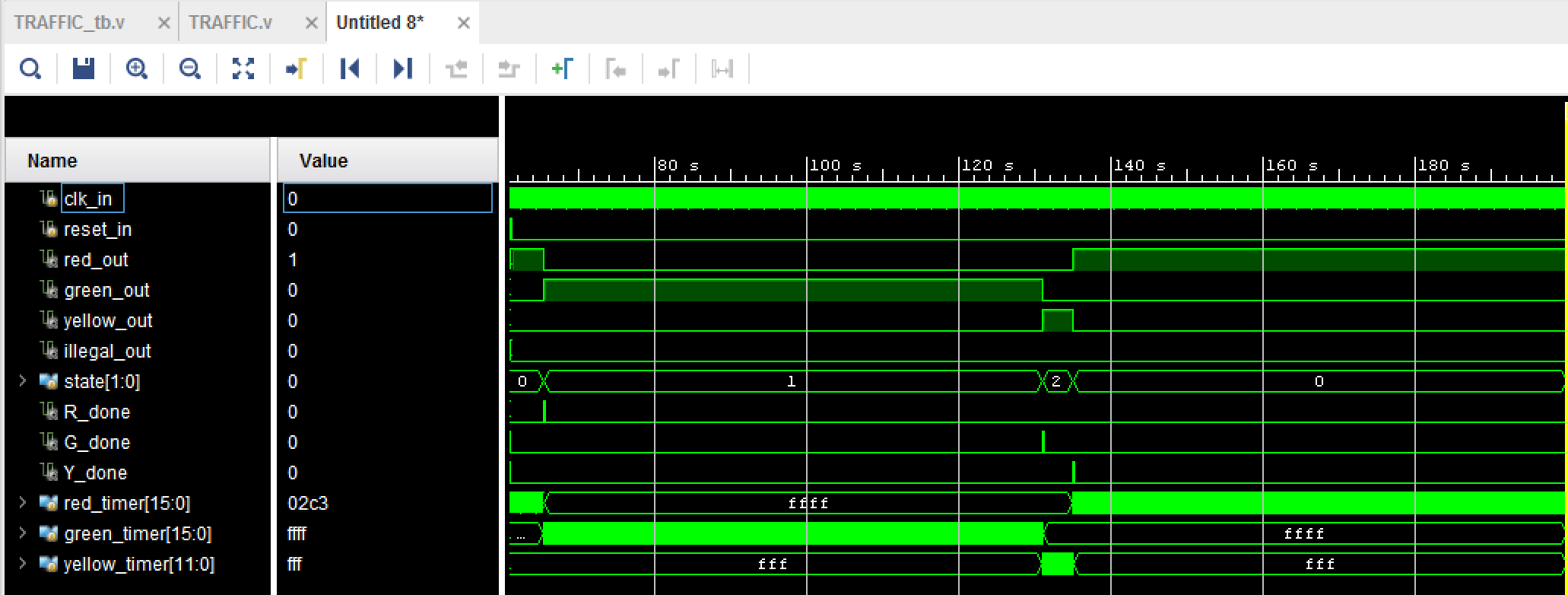
Now let's run the simulation for 200 seconds (change 20 to 200 in the
quick access part and rerun). Then zoom out a bit so you can see 200
seconds worth of waveforms. You should see the following:
You should also take a look at some of the objects in the TRAFFIC.v
source by clicking on "my_traffic" in the "Scope" window and dragging
those signals into the waveform window, and rerunning via the icons.
You can see something like the following, showing how the internal
signals behave. Below you see the state going through its cycle,
the timers running and reset to all 1s, the done lines, and so on.
Verilog Intro
When you learn Verilog, it is helpful to keep in mind that the syntax was invented for simulation
purposes, not for describing programmable logic designs. This will come in handy when learning
about how to code for flip-flops.
    module TOP(A, B, C, D, O);
    input A,B,C,D;
    output O;
    .
    wire A,B,C,D;
    wire O;
    .
    .
    .
    endmodule
and this maps to the following figure:
    module name (
        input A, B, C, D,
        output O
        );
    .
    .
    .
    endmodule
Note that there is no semicolon after "D", just a comma, since it's still within a declarative
list, and no comma after "O", since that is the last element in the list.
    module cname (
        input a, b,
        ouput F
        );
    .
    .
    .
    endmodule
We don't need to know what "cname" does yet, but we do need to know how to
instantiate it inside another circuit (called TOP). Do do that, the syntax is the following:
    module TOP (
        input A, B, C, D,
        output O
        );
    //
    // these are comments just like in c or c++!!!!
    //
    wire c1, c2;
    cname CNAME1(A,B,c1);
    cname CNAME2(C,D,c2);
    .
    .
    .
    endmodule
Note the syntax "cname CNAME1(A,B,c1);". This has the required semicolon at the end. The
first term, "cname", is the name of the module ("module cname(...)" as above). The 2nd
term, here "CNAME1" and "CNAME2" is the instantiation name. This can be anything, it's just
a way of differentiating one instance of a circuit from another. The arguments "A, B, c1"
and "C, D, c2" are names of the cname input/outputs as known inside TOP! This is an
important concept for how to specify the connections: if you use this syntax, then you have
to be careful that the order corresponds to the order inside the module.
    .
    .
    cname CNAME1(.a(A), .b(B), .F(c1));
    .
The ".a" specifies the name of the io port inside the instantiated ciruit, and the "(A)"
specifies what is wired to it. This is nice - it means you can't go wrong! So the overall
Verilog code thus far is:
    module TOP (
        input A, B, C, D,
        output reg O);
    //
    // these are comments just like in c or c++!!!!
    //
    wire c1, c2;
    cname CNAME1(.a(A), .b(B), .F(c1));
    cname CNAME2(.a(C), .b(D), .F(c2));
    .
    .
    .
    endmodule
Wires
Next we have to discuss the Verilog syntax for naming gates. However, this is not
how it works! In Verilog (as is also the case in VHDL, the main competitor), you don't
name the gates, but instead you name the inputs and outputs, and use operators (&,|,^)
for the gates.
To begin, let's take the simple constructs of AND, OR, XOR, and NOT:
    wire A;
    wire B;
    wire C,D,E,F;
Note the important semicolon at the end of each Verilog statement, required just like in C or
C++. (And like C or C++, if you forget the semicolon, you will get an error message in the
compilation that will not say "you left the semicolon off".)
Also note you can have 1 line per wire, or declare multiple instances of wires on the same
line.
Operation Operator
AND &
OR |
XOR ^
NOT ~
    wire A;
    wire B;
    wire C,D,E,F;
    assign C = A&B;
    assign D = A|B;
    assign E = A^B;
    assign F = ~A;
Note the use of the "assign". Recent incarnations of Verilog allows flexibility, and for pure
combinatorial logic implemented in an FPGA by using Verilog (that is, not for simulation),
the assign statement is not needed. So the following is equivalent code to what's just above:
    wire A;
    wire B;
    wire C = A & B;
    wire D = A | B;
    wire E = A ^ B;
    wire F = ~A;
or also equivalent:
    wire A,B,C,D,E,F;
    C = A & B;
    D = A | B;
    E = A ^ B;
    F = ~A;
Now we are ready to write the rest of the code for cname and TOP:
    module TOP (
        input A, B, C, D,
        output reg O);
    //
    // these are comments just like in c or c++!!!!
    //
    wire c1, c2;
    cname CNAME1(.a(A), .b(B), .F(c1));
    cname CNAME2(.a(C), .b(D), .F(c2));

    O = c1 & c2;

    endmodule
and for cname:
    module cname (
        input a, b,
        ouput F
        );
    F = a & b;

    endmodule
assign F = a & b;
The assign statement tells you that whenever "a" or "b" changes, then assign a new value to "F".
And, even more importantly, if "a" and "b" don't change, don't worry about "F". This is a
common thing in Verilog, that some of the syntax is for simulation, and some for what is called
"synthesis", where you turn logic into real gates.
Mux
A mux in Verilog can be pretty simple. As described above
a mux is something that has 3 inputs - S, D0, D1 - and one output, Q. S controls
which of the 2 inputs D0 or D1 gets sent out onto Q.
In general, the syntax is:
assign out = control ? signal1 : signal0;
where "signal1" is what you want to send to "out" when control=1, and "signal0" when control=0.
So for our mux, lets say that when S=0,
Q=D0, and when S=1, Q=D1. The syntax is:
assign Q = S ? D1 : D0;
Busses
Note that a collection of wires can also be a thought of as a single object called a "bus".
This is analogous to a vector, which is an object that has components.
For instance,
let's say that the input wires A and B are 2 bits of a 2-bit wire we can name (arbitrarily)
as N. Then we can declare N as a 2-bit wire via:
wire [1:0] N;
The syntax [1:0] means that there are 2 bits, and they are
labelled as bit 1 and bit 0. You could also use
wire [0:1] N;
but the former is more common (it comes from
having the most significant bit, MSB, specified before the least significant bit, LSB).
Let's rewrite our code above using busses for both A,B and the results C,D,E,F where
A is the LSB N[0] and B is N[1], and etc for C as the LSB of the bus M:
    wire [1:0] N;
    wire [3:0] M;
    M[0] = N[0] & N[1];
    M[1] = N[0] | N[1];
    M[2] = N[0] ^ N[1];
    M[3] = N[0];
Of course the block of code looks a bit more complex than the one above it, but it's just to
illustrate how busses are used.
Registers
Verilog contains one other type of declaration called registers, declared as "reg".
There are circumstances where reg and wire are interchangable, but basically you use "reg"
when you are referring to flip-flops, latches, etc things that can store a result and
keep it until something changes it.
For most of our purposes, we will use reg to mean flip-flops, which means mostly DFF
primitives. To make a reg you simply do this:
reg F;
How you use it is another story, told next.
Flip-flops
Next we need to know how to describe flip-flops, or DFFs from now on. Any DFF will
need (at the very least) a clock (CLK), and input (D), and an output Q, as shown in
Figure 1. Now go back to what
Verilog was originally invented for - simulation - an imagine you were writing code to
simulate a DFF. You could write the code so that at all times, you check on the value of CLK
and of D, and when CLK transitions, you simulate the action of Q goes to D. But you don't
need to check on D at all times, you only need to check when CLK transitions (from low to high
or high to low depending on what you want). In verilog, we would therefore write the following
code for a DFF (CLK, D, Q) that transitions on the positive edge ("posedge") of the clock CLK:
    wire D;
    reg Q;
    always @ (posedge CLK) Q = D;
That's it, the output Q will be the output of a DFF! Verilog allows you do instantiate as many
DFF as you like, and to save you having to write "always @..." every time, you can do the
following using "begin" and "end":
    wire A,B;
    reg C,D;
    always @ (posedge CLK) begin
        C = A;
        D = B;
    end
There, is, however, a catch concerning the state
Q = D.
To illustrate, what if we have the following code:
    wire A;
    reg B,C;
    always @ (posedge CLK) begin
        B = A;
        C = B;
    end
There are 2 ways to synthesize this into gates. In the first way,
we could assume that the first line,
"B = A", means that we want one DFF where at the
posedge of CLK the output "B" is set to "A", and the second line, "C = B", means that the output
"C" is the same as "A". This is akin to what you would do if writing code for a computer,
and will synthesize to the following:

    wire A;
    reg B,C;
    always @ (posedge CLK) begin
        B <= A;
        C <= B;
    end
Non-blocking is the standard way to instantiate flip-flops, and it is recommended that you
just get in the habit of using <= whenever you are dealing with DFFs inside Verilog
always statements.
Creating a Real Circuit
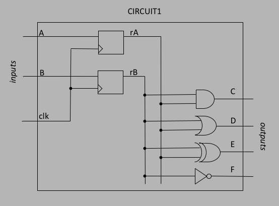
    module CIRCUIT1(
    //
    // declare the inputs and outputs
    //
        input clk,
        input A, B,
        output C, D, E, F
        );

    //
    // register the inputs
    //
    reg rA, rB;
    always @ (posedge clk) begin
        rA <= A;
        rB <= B;
    end
    //
    // conbinatorial logic for the outputs
    //
    assign C = rA & rB;
    assign D = rA | rB;
    assign E = rA ^ rB;
    assign F = ~rB;
    //
    // done!
    //
    endmodule
Note that you have to use the "assign" statement for the outputs.
Verilog FSM
    module TRAFFIC(
        input clk,
        output reg red,
        output reg green,
        output reg yellow
    );

    endmodule
Note that the outputs are all registers. This is because we will have them change state
inside the FSM, so we might as well make them registers since we will want to register the
outputs anyway (as a matter of good form).
    reg [15:0] red_timer;
    reg [15:0] green_timer;
    reg [11:0] yellow_timer;
In our FSM above, we need 3 lines that signal the timers are done for each light:
These can be wires because they will only denote the condition for the timers to be done,
which will be:
    wire R_done = (red_timer == 0);
    wire G_done = (green_timer == 0);
    wire Y_done = (yellow_timer == 0);
Note that these wires are logic levels, and you can think of them as "true" or "false".
The "true" condition here is that the red_timer counts all the way down to 0, so we
use the syntax "red_timer == 0". Note the 2 "==" signs, this is done to distinguish it
from the assignment "red_timer = 0", which would be a syntax error since
we do not assign values to a reg outside of an always block like this.
    always @ (posedge clk)
        if (red) red_timer <= red_timer - 1;
        else red_timer <= 16'hFFFF;
Things to notice here:
As a shortcut, we could implement all 3 timers in the same "always" block like this:
    always @ (posedge clk) begin
        if (red) red_timer <= red_timer - 1;
        else red_timer <= 'hFFFF;
        if (green) green_timer <= green_timer - 1;
        else green_timer <= 'hFFFF;
        if (yellow) yellow_timer <= yellow_timer - 1;
        else yellow_timer <= 'hFFF;
    end
A few things to notice here:
Now that we have the timers taken care of, all we need to do now is
specify the FSM. We will have 3 states (RED, GREEN, YELLOW), so we need
a 2-bit register to hold the state value, and we will use that
register, and the R_done, G_done, and Y_done lines to control the state,
which controls the red, green, and yellow registers that control the
lights and the timer. The code looks like this:
    reg [1:0] state;
    parameter [1:0] RED=0, GREEN=1, YELLOW=2;
    always @ (posedge clk)
        case (state)
            RED: begin
                    red <= 1;
                    green <= 0;
                    yellow <= 0;
                    if (R_done) state <= GREEN;
                    else state <= RED;
                end
            GREEN: begin
                    red <= 0;
                    green <= 1;
                    yellow <= 0;
                    if (G_done) state <= YELLOW;
                    else state <= GREEN;
                end
            YELLOW: begin
                    red <= 0;
                    green <= 0;
                    yellow <= 1;
                    if (Y_done) state <= RED;
                    else state <= YELLOW
                end
        endcase
Things to note:
Putting this altogether, the code will look like this:
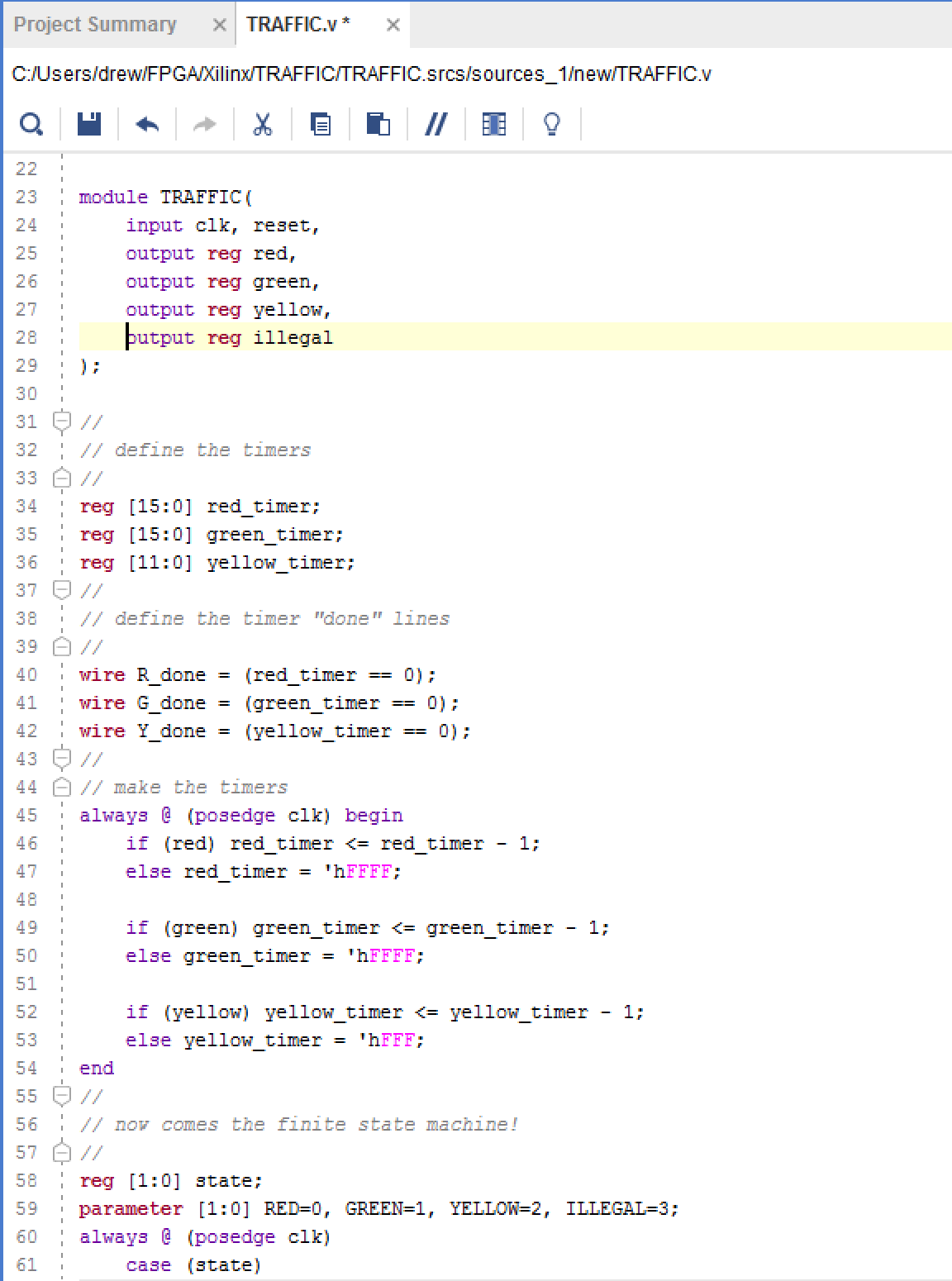
module TRAFFIC(
    input clk, reset,
    output reg red,
    output reg green,
    output reg yellow,
    output reg illegal
    );

    //
    // define the timers
    //
    reg [15:0] red_timer;
    reg [15:0] green_timer;
    reg [11:0] yellow_timer;
    //
    // define the timer "done" lines
    //
    wire R_done = (red_timer == 0);
    wire G_done = (green_timer == 0);
    wire Y_done = (yellow_timer == 0);
    //
    // make the timers
    always @ (posedge clk) begin
        if (red) red_timer <= red_timer - 1;
        else red_timer = 'hFFFF;

        if (green) green_timer <= green_timer - 1;
        else green_timer = 'hFFFF;

        if (yellow) yellow_timer <= yellow_timer - 1;
        else yellow_timer = 'hFFF;
    end
    //
    // now comes the finite state machine!
    //
    reg [1:0] state;
    parameter [1:0] RED=0, GREEN=1, YELLOW=2, ILLEGAL=3;
    always @ (posedge clk)
        case (state)
            RED: begin
                illegal <= 0;
                red <= 1;
                green <= 0;
                yellow <= 0;
                if (R_done) state <= GREEN;
                else state <= RED;
                end
            GREEN: begin
                red <= 0;
                green <= 1;
                yellow <= 0;
                if (G_done) state <= YELLOW;
                else state <= GREEN;
                end
            YELLOW: begin
                red <= 0;
                green <= 0;
                yellow <= 1;
                if (Y_done) state <= RED;
                else state <= YELLOW;
                end
            ILLEGAL: begin
                //
                // this is the illegal state!  turn on the
                // red light and wait for the reset to go high
                //
                illegal <= 1;
                red <= 1;
                green <= 0;
                yellow <= 0;
                if (reset) state <= RED;
                else state <= ILLEGAL;
                end
        endcase

endmodule
Note that we have the "ILLEGAL" state defined. If the FSM gets into this
state, it turns on the red light and turns off the other lights, and waits
for the reset. The state will sit there in ILLEGAL forever until the
reset is asserted. This might not be so great since it means someone (or
something) has to intervene. So, we could easily invent another output,
called "illegal", and have that output asserted
(illegal <=1) when we are in the ILLEGAL
state, so that maybe it will turn on an alarm in some control
room somewhere (or wake up some AI!). Once the reset is asserted,
we have to set illegal <= 0, and transition back into the RED
state and everything should go back to normal.
Xilinx Vivado 2017.2 Introduction


`timescale 1ns / 1ps
In Verilog, the backwards apostrophy "`" denotes a "directive", used
for things like include files, etc. The "timescale" directive
is used to denote the time scale for the simulation, and the
precision. The timescale here is 1ns (the "precision" is 1ps), and
the way that is used is that in the stimulus, if you want to specify
a delay, then if you say "#22" then that means 22ns. The precision
is for the simulator and represents the smallest time you can see
on the waveform. 1ps is pretty precise, and unless you know that
you can simulate things to that level, you should probably change
the precision to 1ns just to save simulation time. But you can also
leave the timescale at "1ns/1ps" and all will be well.
Verilog Testbench
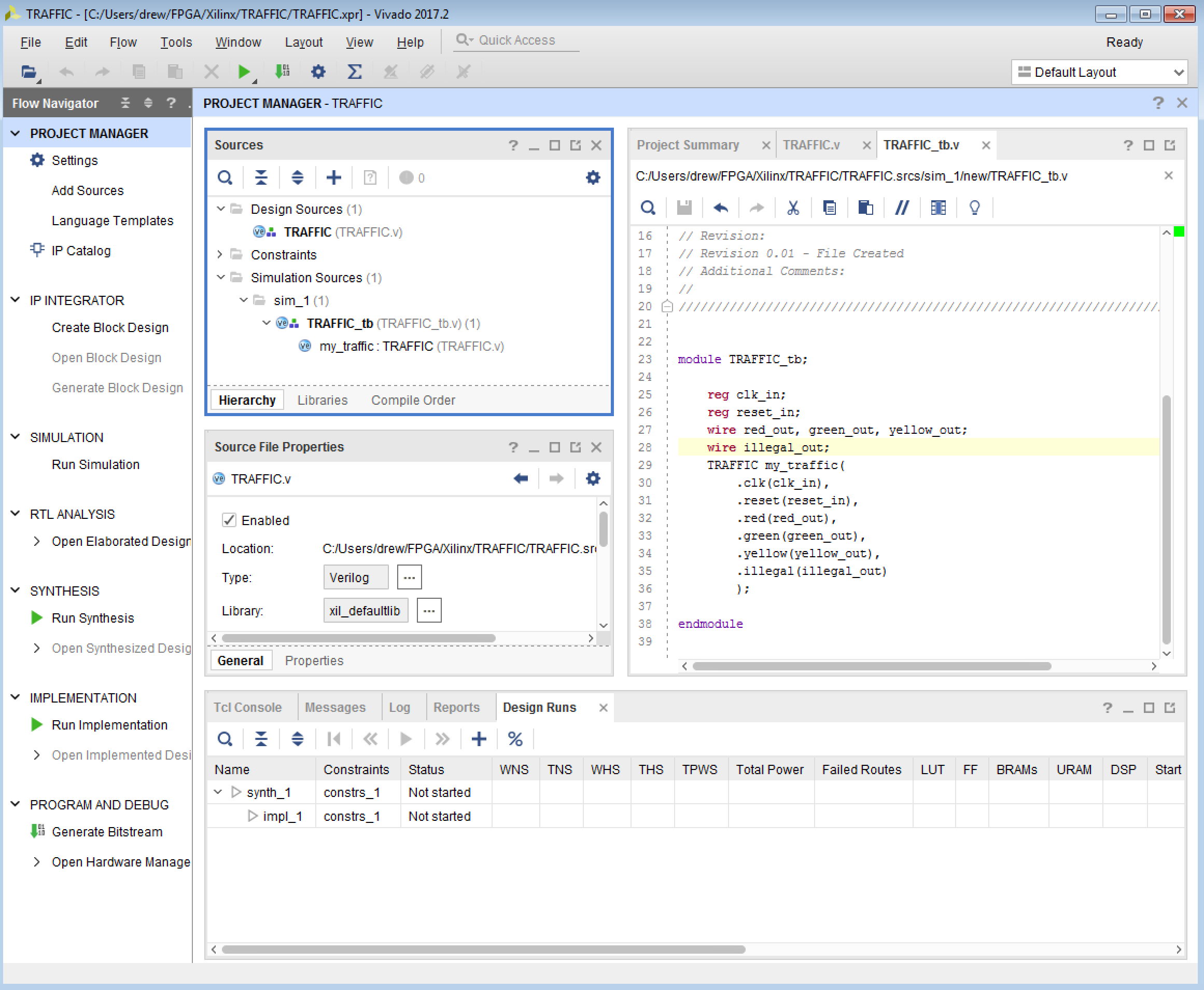
    reg clk_in;
    reg reset_in;
    wire red_out, green_out, yellow_out;
    wire illegal_out;
    TRAFFIC my_traffic(
        .clk(clk_in),
        .reset(reset_in),
        .red(red_out),
        .green(green_out),
        .yellow(yellow_out),
        .illegal(illegal_out)
        )
Paste that code into the file, and
if there are no typo's, it should look like this:

`timescale 1us/1ns
We specify the transitions on the clk_in line by adding the
the following code:
    parameter PERIOD = 1000.0;
    always begin
        clk_in = 1'b0;
        #(PERIOD/2) clk_in = 1'b1;
        #(PERIOD/2);
    end
Notes on the above:
    initial begin
        reset_in = 0;
    end
The Verilog "initial" statement
does just that, initializes things. Since we
set it to 0 and don't change it, it will stay at 0. We of course
do not have the ability with just this code to service a transition
to the ILLEGAL state, but that's ok for now since we don't have the
ability to enter the ILLEGAL state with the stimulus.
    always @ (posedge clk)
        if (reset) ....
        else ....
For asynchronous, it's a bit different:
always @ (posedge clk or posedge reset)
if (reset) ...
else ...
The "or posedge reset" means just that - wait for a posedge of the clock,
OR reset.
    initial begin
        reset_in = 0;
        #100 reset_in = 1;
        #100 reset_in = 0;
    end
This toggles reset_in from 0 to 1 after 100 "ticks" (here microseconds),
and back after another 100.
So for instance, the code in the TRAFFIC.v
file should be changed to:
always @ (posedge clk) begin
    if (red) red_timer <= red_timer - 1;
    else red_timer = 'hFFFF;

    if (green) green_timer <= green_timer - 1;
    else green_timer = 'hFFFF;

    if (yellow) yellow_timer <= yellow_timer - 1;
    else yellow_timer = 'hFFF;
end
we can add the following 5 lines:
always @ (posedge clk or posedge reset) begin
    if (reset) begin
        red_timer <= 'hFFFF;
        green_timer <= 'hFFFF;
        yellow_timer <= 'hFFFF;
    end
    if (red) red_timer <= red_timer - 1;
    else red_timer = 'hFFFF;

    if (green) green_timer <= green_timer - 1;
    else green_timer = 'hFFFF;

    if (yellow) yellow_timer <= yellow_timer - 1;
    else yellow_timer = 'hFFF;
end
You can do the same for the state:
    always @ (posedge clk)
        case (state)
changes to:
    always @ (posedge clk or posedge reset)
        if (reset) state <= RED;
        else case (state)
Now rerun the simulation (it will ask you if you want to discard the old
one, which is ok to do). The problem is sometimes flakey, so you might have
to click on the "quick access" and rerun the waveforms, but after messing
around you should see something like this:
Digilent BASYS 3 Development Kit | Back to top |
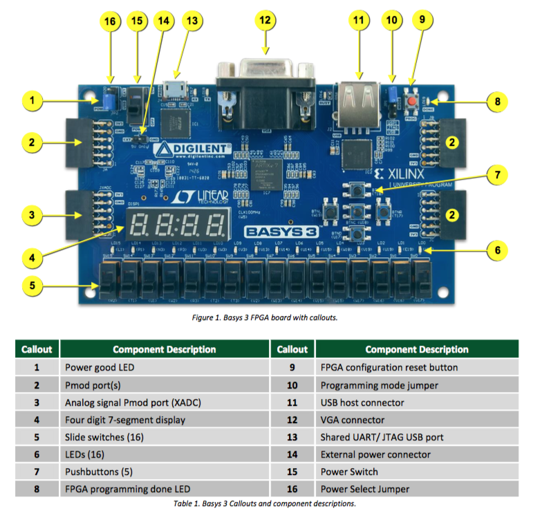
The board consists of a Xilinx Artix-7 FPGA, which has 1.8Mbits of fast block RAM, clock management with PLLs, an on-chip ADC, and can run at up to 450MHz clock speeds.
The board has a VGA connector, 2 types of USB (micro and regular), 5 push buttons, 16 LEDs and 16 switches, and a 4-digit digital LED display. For IO it has 4 "Pmod" connectors, 3 of which are for general IO and 1 has the ADC. It's not a particular powerful board, but is good for learning, and doing simple operations. And once you learn this board, learning more complex ones is easy.
To start, go to the above Digilent web site, click on "Reference Manual", and then click on "Download This Reference Manual". Or you can get it directly from here. That should bring over the file "basys3_rm.pdf", which will become a valuable reference.
There are many other files available on the Digilent web site, with demo projects that you might want to look at once you finish with this tutorial.
The way boards like this work is that the various gadgets (switches, LEDs, etc) are all connected to specific IO pins on the FPGA. Your first project teaches you how to write Verilog code, synthesize it, then have Vivado do what is called "place-and-route" (P&R), and finally download into the chip. Synthesize specifies the logic, what's connected to what, and P&R determines what actual resources will be used and connected. You have to feed Vivado the source code, and the specifics on the IO pins, and it will do the rest.
The first thing we will do is to build a project that sets up a clock
and counters to blink some of the LEDs. Runing Vivado 2017.2, you should see the
same picture as described above. Click on
"Create Project", and go through the "New Project" wizard, and specify a
new project which you can call "blinking". This will be a "RTL Project",
check "do not specify sources at this time", and that will get you to the
"Default Part" menu. Now we have to specify the exact FPGA part we are
using. You can find this in the "basys3_rm.pdf" file on the first page:
XC7A35T-1CPG236C: "XC7A" means Artix-7 model, 35T is the specific
part (the Artix-7 comes in many sizes), the "-1" is a mistake
(it should be at the end of the model, it's the speed designation)
and CPG236 is the "form factor" (this determines how it's attached to the
board). So you should choose "xc7a35tcpg236-1" in the "Default Part"
window and hit "next", and then hit finish. You will get a fresh window
with nothing in it, like what is shown below:
Click on the "+" in the "Sources" panel, "Add or create design sources",
"Create File", call it "TOP", hit "OK", and then "Finish". It will
next ask you to specify IO Ports, just hit OK there and answer "Yes" to
the next question. It will then show you the file "TOP.v" under the
"Design Sources(1)" item in the "Sources" panel.
Double click on "TOP (TOP.v)" and edit the source file. It will empty
except for the `timescale 1ns/1ps directive at the top, some comments
that you can erase or leave, and the module declaration:
We want to blink the LEDs so we can see them. We will do this by defining
a counter, and tieing each LED to one of the counter bits.
Let's say that the slowest LED will blink at around once every 5 seconds,
or 0.2Hz.
Each subsequent LED will blink x2 faster, which gives 0.4Hz, 0.8Hz, 1.6Hz,
etc. 16 bits is quite a large dynamic range, so some of the faster LEDs
probably won't be seen as blinking, but that's ok for a first project.
For a 100MHz clock, each "tick" is 10ns, so we will need $10^8$ ticks to
get something that ticks every 1 second. If we want a tick every 5
seconds, we want something like $4\times 10^8$ ticks, so we want to solve
the equation $2^N=4\times 10^8$, which comes out to $N=28.6". This says
we need a 29-bit counter. So the code will look like this:
Now you are ready to check if the syntax is correct. If you click on
"Run Synthesis" in the left most "Flow Navigator" panel, it will run the
actual synthesis and report any errors. It will first ask you which
"run" you want to launch, just hit "OK" at that first question. You should
see "Running synth_design" with a circling progress indicator
in the upper right hand corner of the window. If everything worked ok,
it should say "Synthesis Complete" with a green check mark, and come up with
a "Synthesis Completed" pop-up window asking you want you want to do next.
Just hit "Cancel" there.
Next we want to specify the IO pins that the code will use for the inputs
and outputs. To do this you first have to find out what pins on the FPGA
they are connected to. For the clock, section 4 of basys3_rm.pdf (page 6)
tells you it is pin "W5". For the reset, let's use one of the push buttons,
which are specified in section 8 ("Basic I/O"), at the top of page 15. If you
look closely at the board, you will see each of the buttons has a label. Of
the 5 buttons, there are "BTNL", "BTNU", "BTNR", "BTND", and "BTNC" for
left, up, right, down, and center. Let's use the upper one, "BTNU", which on
page 15 is at pin T18. Also on page 15 it shows the 16 LED pins (from MSB
to LSB) as L1, P1, N3, P3, U3, W3, V3, V13, V14, U14, U15, V18, V19, U19,
E19, U16. Notice also that the circle shows each LED connected to the FPGA
through a resistor on one side, and ground on the other. This means that
when the FPGA signal is 1, the LED will turn on.
Now we have to set up the source file that specifies the IO pins. This file
is special, and plays a key role in the project. To make it, go back to
the "Sources" panel and click the "+" sign again. In the "Add Sources"
window, change the radio button to "Add or create constraints" and hit "Next",
then click "Create File", give it a name (might as well use the same name,
"TOP"), and click "Finish". Now you have to edit it. In the "Sources"
panel, you should see "> Constraints (1)", click on the ">" and it should expand
and you should see "TOP.xdc". That's the file you want to edit. Double click,
taking you into an empty file.
The syntax is a bit obscure, but the good thing is that once you get it correct
once, you never have to change it! The thing to understand is that you have
to match the pin (e.g. "W5" for the clock) to the IO name in your source (here
it's "clock"). So to do this, type the following:
Next do the same thing for the reset line, and the 16 LEDs. It should
look like this:
Now you are ready to build it. On the left, in the "Project Manager"
panel, you will see "IP INTEGRATOR", "SIMULATION", "SYNTHESIS",
"IMPLEMENTATION", and "PROGRAM AND DEBUG". Under them are the
operations you can click on. If you click on "Generate Bitstream"
under "PROGRAM AND DEBUG", it will realize that you've not
run the synthesis or implementation stage, and will ask you if
you want to do that by putting up a pop-up window that will say
something about how the "Synthesis if out-of-date" and ask if you
want to run both synthesis and implementation. Say "Yes", and
it will probably put up another window called "Launch Runs". Say
"OK" to that one as well. It will then run the synthesizer,
followed by the place-and-route, if there are no errors, and
then it will make the "bit file". This is a file that can be
downloaded to the FPGA over USB.
Now go back to the documentation basys3_rm.pdf, and look in section
2 "FPGA Configuration". It details 3 ways to program the board:
using a serial protocol called "JTAG", storing a file in the SPI
flash chip, or transferring from a USB memory stick. We want to
connect our FPGA to our computer using the USB connection, and
program using JTAG. To do this, look for the 4-pin jumper to the right
of the USB connector (upper right when holding the board so that
the VGA connector is on the upper side) called JP1. It will have
4 pins and a blue jumper. You want to make sure the blue jumper
is connecting the middle 2 pins together.
Next, to make sure that the USB will work, you have to look for
the 3-pin jumper JP2 and set it to "USB". This will tell the board
to draw its power from the USB connection, and you have to make sure
that you are using the microUSB connector right next to the on/off
switch. Now you are ready to connect the board to your computer
via USB.
Back to Vivado, if all is well you should see a popup window called
"Bitstream Generation Completed". It wants to know what you want
to do next. Check "Open Hardware Manager" and hit OK. That will
open up the "Open Hardware Manager" tab on the left panel, and under
it you should see "Open Target". Click on that and click on "Auto Connect"
when you see that option. If all goes well, the "Program Device"
option should now be clickable. When you click on that, it will tell
you the devices you can program, which should be your xc7a35t chip.
Click on that. It will bring up a window with the name of the bitstream
file you made. Click on "Program", and if all goes well you should
see a window with a green progress bar. After that, the FPGA will be
programmed and you should see the LEDs flashing. Congratulations!
Note that the LEDs to the left are blinking slowly, and the LEDs to
the right are not blinking at all. In fact, they are, but they are
blinking so fast that you can't see them turn off, so they look like
they are all on all the time. If one of the LEDs is off all the time,
then either you have a mistake in the xdc file for that LED signal,
or the LED is probably just busted. The former is much more likely!
Don't forget to try pushing the reset button to make sure that is
working properly as well.
The next project consists of code that will count the number of
times some input was present, and present the counter in the
4-digit LED display. For the counter, let's count the number of
times one of the push buttons are pushed, let's put the count
as a binary digit in the LEDs, and display the number of couts
in the LED display.
For the input, we use the bottom push buttons for counting, and leave
the top for the reset.
To set any individual digit, you drive one of the 4 select lines AN0, AN1,
AN2, or AN3, and then drive the 8 lines CA, CB..., DP. Let's name
them DIGIT[3:0] for the 4 select lines, SEGMENT[7:0] for the 7 segments
of the digit, and DP for the dot LED. The following are the xdc
constraints for this, plus the other things needed:
Your verilog TOP module will need to have the
inputs clk, reset, btnCnt, and the outputs
digit[3:0], segment[6:0], dp, and LED[15:0], so the module
declaration should look like this:
To display 4 different numbers in the 4 different digits, what you
have to do is to store the 4 numbers in registers, and then loop
over the 4 digits, sending the stored number to the segments one
at a time. This has to be done with a clock fast enough so that you
don't see "flickering".
The following code can be useful in changing a 4-bit number (hex
numbers are all 4 bits, 0-15) into the right combinations of
segments to display the number. The inputs are a clock (used to
clock data into registers so that it's in memory), a 4-bit number
("number[3:0]") and the corresdponding 7-bit segment pattern cooked
up so that the numbers 0-9,A,B,C,D,E,F appear. This of course
means that the displayed 4-digit number will be in hex.
Now we need a circuit that will input a 4-digit hex number
(number[15:0]), and with a clock loop over the 4 digits,
sending each of the 4 digits to the segments one at a time.
The module name here will be called display4.v, and will
have the following IO ports:
First off, we define the 16-bit count register as before, and this
will go into the LED block. We also define 4 count digits, each one
is 16 bits to it holds a full digit:
Inside the always block where we increment "the_count", we add the following:
Now we are ready to put all the code together into a single TOP.v. It
should look something like this:
Now you have to build the code and download into the FPGA. The first step is to
run the synthesis tool. What synthesis does is to look at the code, decode it
into logic and flip-flops, and set up a list (called a "netlist") of what is
connected to what logically. In the "PROJECT MANAGER" window to the left,
which should look like this:
click on "Run Synthesis", under the "SYNTHESIS" tab. It might ask some questions,
just say yes and go on. You should see "Running synth_design" in the upper right
hand corner, plus a circular progress widget spinning.
If there are no code errors, the synthesis will pass, and you will get a window
asking you what to do next. It will look something like this:
When implementation is finished, you should see another window pup up. Click
on "Generate Bitstream" and hit OK. This will make the file of bits that will
actually get downloaded into the FPGA. You will see "Running write_bitstream"
in the upper right corner of the Vivado window.
Once that is finished, you will see yet another window. Click on
"Open Hardware Manager" and hit OK.
Now you have to connect to the basys3 board over USB with the micro-usb
cable plugged into the port near the power switch. You should see the
LED above the word "POWER" light up. Vivado has to now connect to it,
and you do this by clicking on "Open Target". If this is the first time you
are connecting after a powerup, clicking on "Open Target" will show you a
popup window. Click on "Auto Connect" as shown below.
You should see a brief flash from a progress bar, and then the following in
the "HARDWARE MANAGER" panel (top, next to "PROJECT MANAGER"). It should
show that the localhost is connected. Then click on "Program Device". It
will open up a little window with "xc7a35t_0" as the only option, which is
the basys3 board. Click on that. Now you have to specify the file you want
to download. You should see a "Program Device" window pop up, like this:
Make sure that "Bitstream file:" is set correctly, it should point to a
subdirectory in the directory you are working. If it's not correct, navigate
there. The .bit file is in "../counting.runs/impl_1" where "counting" is
the name of the main subdirectory I'm working. Find the file, hit "Program",
and it will send the program to the FPGA and run it. If the JP1 jumper is
set to "JTAG", you should see 0000 on the display. Hitting the bottom
push button of the 5 (in a cross pattern) should increment it.
As discussed above, you can send the program into the onboard flash ram,
so that the board will power up and load the program automatically.
To accomplish this, first move the jumper on J1 to the QSPI position
(see Basys3 photo above, J1 is item 10,
the jumper should connect the first
2 pins closest to the edge).
The file that is sent to the flash over the USB cable is a .bin file,
and has to be created when you "Generate Bitstream". To ensure this,
right click on "Generate Bitstream" and select "Bitstream Settings".
That will produce a popup window that looks like this:
Click on "Bitstream" in the left panel "Project Settings", select
"-bin_file*", and hit OK. Then generate the bitstream. It should
make the *.bin file, in the same place (*_runs/impl_1/*.bin)
as the *.bit file.
Now you have to tell Vivado about the flash memory, so it can download
to it. The easiest way to do this is to click on
"Add Configuration Memory Device" in the hardware manager and select
the device "xc7a35t_0"
This will bring up a new window called "Add Configuration Memory Device":
In the "Search:" text area, type in the flash device name, which is
found on page 6 of the basys3_rm.pdf file: S25FL032. That should bring
up the correct name in the list below the search field. Click on that
name and hit OK. If all is well, you should see something like this
in the "Hardware" panel:
Then all you have to do is right click on the memory part
(s25fl032p-spi-x1_x2_x4) and select "Program Configuration Memory Device".
It will pop up yet another window asking for the .bin file. Navigate
to it in the "Configuration file:" text window (again, it's in the
directory *.runs/impl_1 where * is the project name), select the .bin
file, and hit OK, and hit OK again in the "Program Configuration Memory Device"
window. It will then show a progress window where it first erases, and then
programs the flash. It will take probably 30 seconds or so, and if all
goes well will show a window that says "Flash programming completed successfully".
Hit ok.
The last thing you need to do now is to actually load the program from
flash into the FPGA by pushing the "PROG" button (item 9 in
the Basys3 photo above). It takes about 5
seconds.
Having an FPGA in a development kit like the BASYS3 can be very useful if you
are planning to use it for data acquisition. And to do that, we need some kind
of communication path between the FPGA and a computer. The BASYS3 does have
2 USB connectors: a micro-USB on J4 and a macro-USB (standard USB connector)
on J2. The latter is not really useful for I/O, it's more intended to be
used for connecting a mouse or keyboard (see page 7 of
basys3_rm.pdf for more).
The micro-USB connector (J4) is the one we will focus on. The board
side of this connector has a chip that bridges USB to a serial port,
the chip is from a company called FTDI (
Future Techynology Devices International
Ltd), which specializes in gadgets that allow you to use USB connections for
various products. The chip on board is the FT2232HQ USB-UART bridge, and
the data sheet can be found
here. Basically, what it does is to allow you to connect using USB,
and "tunnel" serial port data through to the FPGA. So the communication
path between the PC and the BASYS3 board is via a serial connection, tunneled
inside USB.
The communication path is as in the next figure:
One of the easiest ways to communicate with hardware (like FPGAs) is via
serial communication links. This is quite common for computers, with many
protocols to choose from, all more or less the same. The one we will use is
called RS232, which traces its orgin back to the 1960s.
Serial links such as UART/RS232 are very simple:
a single line carries receive, and another single
line transmit (all of this is from the point of view of the gadget that
does the receiving and transmitting). On page 7 of basys3_rm.pdf you can
see figure 6:
This figure shows the 2 lines serial lines that are connected to the FPGA on
pins B18 (receive) and A18 (transmit).
All you have to do is route these into the FPGA by adding the following the .xdc file:
Then in the FPGA, we will use the wires "RsRX" for receiving data from the outside
world, and "RsTx" to send.
Decoding and encoding RS232 is simple once you understand the time structure.
Let's consider the RsTx line first. This line is the transmitter, from the point of
view of the FPGA. Don't get confused by the figure just above, which labels it
"RXD" in the figure - that is because the whole concept of transmitter and receiver
is relative to which chip is transmitting and which is receiving, as shown in the
figure below.
In all serial links, the information is sent one bit at a time. From the point
of view of the receiver, it has a single line, and on this line it needs to know
when data is coming, what the time period is for each bit, and what protocol it
has to use to decode the data. So the transmitter and receiver have to be in agreement.
For RS232, we have the following rules:
For this project, we will use a serial receiver and transmitter that will use 1
start bit, 1 stop bit, and no parity, and will send 1 byte at a time. You can write
your own verilog to implement this, but if you want to use one that has been
debugged, you can find them below with explanations of how to use them.
Inputs are:
The final bit of code inside your top level module to instantiate
the uart_tx will look something like this:
The way the uart_tx module works is that the line i_Tx_Serial is active low,
so it starts out high. The state machine will wake up when
i_Tx_DV is asserted, and drive o_Tx_Active high.
It then sends the start bit by driving i_Tx_Serial
low for some number of clock cycles determined by the input i_Clocks_per_Bit,
then will send each of the 8 bits by asserting
i_Tx_Serial as appropriate for i_Clocks_per_Bit
clock cycles each. After that it will
drive i_Tx_Serial high for i_Clocks_per_Bit clock cycles,
which would be interpreted
as the stop bit, and finish by asserting o_Tx_Done for 1 clock cycle
(10ns), and drive o_Tx_Active low. The transmission is finished.
As an example, say you want to send the bit pattern 'b11010101 (0xD5) with
a baud rate of 57600 (one of the standard baud rates from the old days). The
whole transaction should look like the following figure, which each bit
being 1/57,600Hz = 17.36$\mu$s long:
Inputs are:
The transfer will be initiated when the i_Rx_Serial line transitions to low
(active low), causing the state machine to latch each serial bit starting with
LSB and ending with the stop bit, after which it will assert o_Rx_DV to indicate
that it has new data for you to use.
Both of these verilog modules were from opencores,
but needed a few changes in order to work. The code above have been tested and verified
inside the BASYS3 board.
To make it easier, the following code (available here)
can be used as a serial I/O driver for your
FPGA:
Your top level module that drives this code might be something like this:
To be clear, CLOCK_DIVIDER is a parameter you set inside your top level,
and pass to the SerialIO module as parameter CLKS_PER_BIT, which puts
it into a 15-bit wire and sends it to both uart_tx and uart_rx.
What follows is a simple straight-forward example of how to use the BASYS3 board for
serial IO. The data that we will send from the BASYS3 will come from the
first 8 bit switches, and the data received will be displayed on the LEDs.
All data will be transmitted as serial IO, 8 bits of data, 1 start and stop bits,
at 1 Mbaud.
The LEDs and bit switches are routed to the FPGA on pins detailed in
the user manual basys3_rm.pdf on page 15.
The relevant figure is reproduced below:
As you can see, the LEDs are driven by the FPGA output through a
resistor to ground (current limiter),
so they are active high (drive it high and it will
turn on). The switches connect the FPGA to 3.3V through a resistor,
so off = 0 and on = 1 (if you hold the board with the VGA connector
up, the switches are down = 0 and up = 1). The pins are shown in
the diagram. We want to drive 8 LEDs (actually 9, we will use one
for a "ready" signal) and 8 switches,
which means you have to add the following to your .xdc file:
To connect the switches and LEDs to the SerialIO module, you would
do something like this:
The line wire [7:0] tx_data = sw ties the input switches to the
SerialIO transmission byte (since we only enabled 8 switches, you
don't have to tell it sw[7:0]), and the 2 lines that begin with
assign tie the LEDs to the ready and received data byte.
Receiving happens asynchronously - that is, the module looks at the
receiving line (RsRx above) and waits for a transition (high
to low). When that happens, it decodes the incoming byte and displays
it on the lower 8 LEDs. Transmission, however, has to be
initiated, so we use one of the push buttons, which is what
pb_down is connected to.
The push buttons are
"debounced" on the board but if your finger bounces it, you will get
many transitions, so it's best to use a decent debouncer inside the
FPGA so that your coffee intake won't cause more transitions.
A common debouncing technique (different that the one above) is to
use the push button to trigger some logic that starts counting.
When the count is up, it looks at the push button again, and if it's
still pushed, it figures that you meant it to be pushed, and that
if it was bouncing while it was counting, it won't worry about it.
You can find such a module called PB_Debouncer.v
here. The inputs and outputs of this
module are:
You wire the line i_PB to one of the push buttons on the BASYS3
board, and look at any of the 2 outputs
o_PB_down and o_PB_up to decide if the button is pushed.
Probably best to look at o_PB_up, because that will be asserted
once the push button is released. This of course implies that you push
and release to initiate something, like a serial transmission out of the
FPGA.
The Xilinx Vivado 2017.2 zipped project "USB_Serial1" can be found
here.
Putty is the name of an all purpose serial port terminal program that
has mostly outlasted its usefulness since the early 2000s. But for us,
it can work to make sure that we have a good communication path to the
BASYS3 board, for both transmitting and receiving. You should be able
to download putty onto your PC (running Windows of course).
To use it, first make sure that the FPGA on the BASYS3 is programmed
correctly. If you use the above project "USB_Serial1", you should see
1001 on the 4 digit display, and then you can run putty.
You should see the following window appear:
If you don't see that window, you should see the "Category" panel on
the left, click on "Session". Then in the panel on the right side,
click on "Serial". You should set the speed to 1000000 (the default
baud rate in the FPGA code, or whatever you might have changed it to),
and the Serial line to something that depends on your computer.
This is where putty can be a pain - it does not necessarily know which
COM port the device manager has mapped the USB connection to. You can
look in the device manager to find out however by right clicking on the
"Computer" desktop icon, and clicking on "Device Manager" for Windows 7.
Then open up the "Ports (COM & LPT)" to see what's there. You should
see something like this:
I don't know why there are 2 USB Serial ports open, but one of them
will work and the other won't (in this example, COM4 works but COM3
does not). Hit "OK" and you should see a blank terminal window pop
up, like this:
Having an FPGA that can be used for acquiring data is a powerful thing,
and at this point you should have a pretty good idea as to how to write
FPGA code and make it work.
But you have to know how to get data into it (other than through the
serial interface, that is). And by data, that means
both digital and analog.
The BASYS3 board has, in addition to the
push buttons, switches, and LEDs, 4 rectangular connectors called
"PMOD connectors". These are shown as items 2 and 3 in the figure on
page 2 of basys3_rm.pdf,
or in the figure
above. The 3 connectors labeled "2"
are general purpose
digital IO blocks that can be used for any kind of IO supported by
the FPGA (even differential). The connector labeled "3" can be used
for either digital or analog signals that are digitized inside the FPGA.
Page 17 of basys3_rm.pdf details how
to use the digital IO blocks. The 3 "PMOD" connectors are labeled
either "JA" (upper left), "JB" (upper right), or "JC" (lower right),
and all conform to the following diagram (also on page 17):
If you look on the BASYS3 board itself, you will see clearly the
label (JA, etc) and where the pin labeled 1 starts: it is always
on the top on one edge, whereas the 3V output is pin 6 on the other
side on the top. All you have to do is route your digital signals
into the right input and connect the port to the FPGA in the
xdc file. For example, the diagram shows that for JA, pin 1
(labeled "JA1") is connected to pin "J1" on the FPGA. That means
you have to specify "J1" in the .xdc file. The following is an
example of connecting all pins in JA to the FPGA and referring
to them in the top level verilog file as an 8-bit bus called
"JA". The xdc code looks like this:
and the verilog input looks like this:
LVDS is a low voltage differential standard that is very commonly
used. Wikipedia has a pretty good page explaining it
here, but basically instead of switching voltage on a single
wire, in LVDS you switch a small amount of current, nominally
3.5mA. The thing is differential, and you have to terminate by putting
a resistor across the inputs usually. The voltage swing is around
800mV, so if you terminate the far end of the differential cable with
$100\Omega$, then you will draw 8mA of current.
Outputing a digital 1 means 8mA of current goes from plus to minus,
and vice versa for a digital 0.
On modern FPGAs, like the Artix7 in the BASYS3 board, the IO pins
can be configured for a host of different IO standards, but for
differential signals, they specify which pins are "paired".
This information is sometimes difficult to find, so it is
provided in the txt mapping file
here. You have to search
for the pins that are paired and set things correctly in the
.xdc file. For instance, say you want to input a differential
signal into the BASYS3 on JA using pin 1 and another pin.
Pin 1 is JA1 in the diagram, and that's pin "J1". In the
above file, you look for "J1" in the left column, and it is
found on line 116:
The pin name is "IO_L3N_T0_DQS_AD5N_35", so you search for the
pair with the name "IO_L3P_T0_DQS_AD5N_35" (note the difference,
"IO_L3N..." and "IO_L3P...") and you can see that that's on pin
"H1", right above (line 115), and "H1" is tied to "JA7", which
is pin 7 on connector JA, which is right below "JA1". No
coincidence! That makes it easy to drive a differential pair
in this block.
In the .xdc file you add something like the following for those 2 pins:
The IO standard is 2.5V, and the port name will be "lvds1_p" and
"lvds1_n". In your toplevel verilog, you would then add the
following to turn that into a single ended digital signal that
you can use in the code:
The Artix7 FPGA version on the BASYS3 board (XC7A35T) contains analog-to-digital
(ADC) circuitry that allows it to monitor various temperatures, voltages, and
other things needed to know how the chip is working. You can access this
circuitry to input an analog voltage, either directly through dedicated analog
input pints, or through IO pins that can be used for either analog or digital.
The ADC circuitry is extremely complex, but for simple slowly changing analog
signals, is extremely useful. The technical details are patented, and Xilinx
is not keen on disclosing, however it is described in some detail in a
Google Patent here (but good luck
in digging out too much details, it is a patent so difficult to read). The
circuitry is available in many of the Xilinx chips other than Artix7, and is
called an "XADC" block.
The Artix7 we are using contains 1 XADC block,
which has 2 12-bit 1 MSPS (mega samples per second) ADCs, and an on-chip
analog multiplexer so that you can route 17 different inputs into the ADC.
The amplifiers support unipolar, bipolar, and differential inputs. For
more technical information on how to use it, see the Xilinx app note
ug480_7Series_XADC.pdf.
These ADCs can be used for various things like temperature monitoring,
or even DAQ for externally driven circuits. In fact, if you don't use
the ADC in your design, it then automatically digitizes all on-chip
sensors for readout over the serial JTAG interface (this is described in
the above document). The internal XADC can convert signals from:
The JXADC header is the one next to the 4 digit display,
and they are paired (positive/negative)
such that the positive pin is on the top row and the negative pin is on the
bottom row in the same column.
The XADC can measure unipolar ($0\to 1$ volt) or bipolar ($-0.5\to +0.5$ volt) signals.
The figure below comes from page 30 of the
XADC manual):
We will be using unipolar mode, and the BASYS3 board only wires up the
dual analog/digital inputs to the FPGA, so we will only be using the
"VAUX" inputs. That means that the input impedance of our XADC will
be around $10k\Omega$, and the sampling capacitor will be around $3pF$,
giving an RC chargeup time of around $30ns$. Note that in unipolar mode, there are 2
switches that connect the positive and negative sides of the sampling capacitor to the
inputs. They are labeled $V_p$ and $V_n$, which are the dedicated analog inputs,
but it is the same for the "VAUX" inputs that we will use via "JXADC" header.
The way the XADC works is typical of analog-to-digital conversion circuits.
A "sample and hold" capacitor is charged up by virtue of an incoming voltage
signal, and this is usually gated so that you can control when it charges.
Charging is the "sample" phase.
Once it is charged, it is disconnected from the inputs, and the voltage will
hold while the signal is being converted from a voltage into a digital
number. This is the "hold" phase. Ideally you want the capacitor to be
small enough so that it charges up fast, but not too small such that any
stray capacitance can compete. And you want the input impedance to be such
that the RC time for charging ($\tau = RC$) is small. Often you will see
ADCs that first charge, and then hold and convert, doing them serially,
which puts a big burden on the front-end analog circuitry to charge up
quickly (so that the overall data rate can be large).
What the Xilinx XADC
does, instead, is to have two sample and hold capacitors like in the figure.
So the XADC can sample and convert simultaneously.
The ADC itself is 12 bits. This means there are $2^{12}=4096$ possible
values, and since the maximum voltage is $1.0$ volts, that means that
the LSB is $1/2^{12}=0.244$mV, which means the precision is around
half that, or $\delta V = 0.122$mV. The rise time of the voltage on the sampling
capacitor is given by $\tau = RC = 30ns$, which means that the voltage
on the capacitor $V_c$ increases with time according to:
$$V_c = V_{in}(1-e^{-t/\tau})\nonumber$$
If $V_{in}$ is the maximum $1.0$ volts, then we can calculate the
time $t_{\delta}$ (or the number of RC times $N\tau$) that
it will take for the signal to get to within $\delta V$ of $V_{in}$, so
that the charging does not dominate the precision:
$$V_{\delta}=V_{in}(1-\delta V)=V_{in}(1-e^{-N})\nonumber$$
which means $\delta V=e^{-t_{\delta}/\tau}$, and solving for $t_{\delta}$
gives
$$N\tau = -\tau\ln\delta V = 9.01\tau\nonumber$$
For $\tau=30ns$, that means we would need around $270ns$ of charging
so that our precision is not dominated by the charging time. The XADC
will run at 1M samples per second (1 MSPS), or $1\mu s$, with parallel
sampling and conversion, so charging will not be a problem, but you should
keep this precision in mind in case you use it at a slower sampling rate.
Using the XADC with VAUX inputs to measure voltages that change on a time
scale longer than the $1\mu s$ operation time will work great, even if we
are not controlling the conversion with a "trigger", something that synchronizes
conversion with the incoming signal. However, if you want to use the XADC
to measure voltages that are changing fast with respect to $1\mu s$, you have
to build a preamp that will integrate the signal using a differential
amplifier with a capacitor as feedback. This is the subject of another
course.
The figure below details the timing of the XADC internals:
A full cycle of conversion takes 26 ticks of the internal clock called ADCCLK, which is derived
from the input clock .dclk_in. Setting configuration register 2 allows you
to determine the ADCCLK frequency.
The documentation is a bit fuzzy, but there was a
technical note
that says the ADCCLK has to be between 1 and 26 MHz if you want to run the ADC at the maximum
1 Msps conversion. For our purposes, we will use the on board 100MHz clock, divide
it in half to get 50MHz, and use that as
input .dclk_in, so our divider will be 2 (see table above), and we will have a 25MHz
ADCCLK which will set the conversion rate to $R=25/26=961.5$ksps.
By using a 50MHz .dclk_in, some of the timing pulses (described below) will be
~20ns wide, which means we can use the 100MHz clock to run state machines and branch
on pulses without encountering race conditions (this is probably overly cautious!).
The conversion period includes all of the time it
takes to assemble and latch the output bits so that they become available
to be latched inside the FPGA by your code.
A good reference for different ways to use the XADC is available
here.
The ADC allows 4 ticks for the capacitor to fully charge and settle,
and can be increased to 10 (see documentation). There are 2
sample-and-hold capacitors, so that one can be charging up
while the other is being digitized.
As you can see in the diagram, .eoc_out is asserted on every conversion,
so the .eoc_out for channel "N-1" in the diagram is the second one asserted
in the diagram, which happens when channel "N" is being converted. Below we
show the logic analyzer output for the XADC.
The ADC on the Artix7 can be configured so that you can trigger it from an
event, or you can enable it by controlling the input enable (.den_in,
short for "data enable in"),
or you can just let it run free and keep digitizing the analog signal you
are sending it by tying the .eoc_out signal, which is a 1 clock tick signal
meaning "end of conversion", to the .den_in signal. This is how we will use
it to build the voltmeter.
A caveat is that if the signal is rising during the time you are digitizing,
you might not get the full value of the voltage, but if your voltage is DC
(or changing slow compared to $1\mu s$) then you won't notice this.
If your signal has a significant AC component however, this can be handled by using the
XADC in event mode instead of the continuous mode that we will be using.
All of this is detailed starting on page 73 of the
XADC manual.
The input voltage to be converted has to be between 0 and 1.0 volts (for
unipolar mode), and the ADC produces a 12 bit number in the upper 12 bits
of the .do-out bus. The resolution of a single bit (LSB) is therefore
$\delta = 1V/1^{12}=244\mu V$. Bipolar mode is more complex and won't be
used here.
The hard part in setting this up is in generating an instantiation of
the XADC into your verilog code.
You can go ahead and do it by hand by
clicking on "Language Templates" under "PROJECT MANAGER", then
click on "Verilog/Device Primitive Instantiation/Artix-7Advanced" and
you will see "Xilinx Analog-to-Digital Converter (XADC)". If you
click on that you will see an example instantation in the right panel.
Cut and paste to your top level file.
However, you will find that for complicated things like XADC, it is
often better to run a "Wizard" and let Xilinx do it for you. This is
the approach we will take here.
To start, click on "IP Catalog" under "PROJECT MANAGER" in the
left panel. It will bring up a new window in one of your panels,
with a tab labeled "IP Catalog". It will look something like this:
Type XADC into the search window, and it should find the "XACD Wizard".
Double click and it will run the wizard, you should see something
like this to begin:
You will see a text field called "Component Name" and you will see
"xadc_wiz_0" in that field. That's fine, it is just the instantiation
name, and will show up with this name in your verilog sources panel.
Underneath "Component Name" you will see 5 tabs labeled "Basic",
"ADC Setup", "Alarms", "Single Channel", and "Summary", and these
are used to set up the instantiation. Here's what
is recommended for each of these tabs:
Click "OK", and you should see a popup window that asks if it's ok to
create a new directory to house all of the new files. It should be
in your project directory. Click "OK". It will then pop up a window
labeled "Generate Output Product". Click "Generate", it will initiate
some activity, and at the end will inform you that it did what it was
supposed to do. Click OK.
Now you should see a new source appear in the same panel with the other
sources, and it should look something like this:
If you open up what's below "xadc_wiz_0" you should see a file called
"xadc_wiz_0 (xadc_wiz_0.v)". That's your source file, it contains
the instantiation of the XADC. You can double click on it, and you will
a huge number of lines. Don't worry, all we have to do now is
instantiate xacd_wiz_0 and that module will do all the heavy lifting.
To instantiate you should place the following template in your code:
This instantiation will produce a series of configuration registers that
control how the XADC works. The configuration registers can be written to
and read from using the DRP (Dynamic Reconfiguration Port), which we will not
use. But it's good to see how these registers are configured, as depicted
in the list below (which comes from the verilog instantiation):
The next project will be to put a DC voltage into the VAUX inputs, use the
XADC to digitize the voltage, and then both
display the result on the 4-digit LED display and transmit via serial port
to a computer (if it's listening!).
We will instantiate the XADC in continuous mode, and tie .eoc_out into .den_in,
and will use pins 1 and 7 of JXADC (corresponding to VCAUX6, FPGA pins J3 and K3)
for the input voltage, which should be between 0 and 1 volt.
We will run the ADC in single channel continuous mode and look at an input
voltage on VCAUX6. The code up the top level to have 4 push buttons: \
one to reset the flip-flops (btnR),
one to trigger the latching of the ADC value (btnL), one to transmit the
ADC value to the PC that will be running a Python script (btnC), and
one to display the version number on the LED display (btnU). The inputs to the
top level will look like this:
We will also make use of the serial transmit (Tx) line (we don't need to
receive anything in this project),
the 4-digit LED display, and the JA, JB, and JC headers to bring signals out
for debugging with a logic analyzer. We will use the 5 push buttons for the
following functions:
Be sure to push either L to latch an ADC value, or D to latch a switch value,
to transmit.
Push button D is used to send a test byte to the computer using the right
most switches. If you use putty (see below), and put a 0x30 on the switches,
it should receive and display a "0" (this is the unicode translation of 0x30).
After the inputs in the verilog code for top.v, we will define 2 parameters:
Next comes code that will produce two clocks: a 50MHz and slower $\sim 3$kHz clock
(not used here). These clocks are put into clock buffers (BUFG),
which are dedicated lines
inside the FPGA that allows faster clocks with a more controlled impedance.
The code for "ClkSynth is straigtforward consisting of a divider using
DFFs, and can be accessed here.
Next we have 4 debouncers and the reset line. We tie the input
"btnR" directly to the "reset" line, and debounce the other 3 buttons
(btnU, btnL, btnC, and btnD) so
that we don't have any human-induced jitter using the same debouncer code
PB_Debouncer as detailed above.
Next comes the XADC instantiation. The ADCs are run continuously, and we
use the .drdy_out signal (called "adc_data_ready" in the code) to latch the
upper 12 bits of .do_out into a 12-bit register called "r_adc_data".
That way, when we want to latch the last legitimate ADC value, we can latch
it from "r_adc_ready".
Just to see how things are going, we can put r_adc_data onto the 12 lower
LEDs via:
The following code implements this:
Notice that the XADC is instantiated using the IP XADC wizard, which should
appear in the project as xadc_wiz_0.
Next comes the code to transmit data to the PC through the serial IO
module. Since we can only transmit 1 byte, or 2 characters, at a time,
we will just use the upper 8 bits of "latched_adc". The code looks
something like this:
Next comes the 4-digit LED display, and the debug signals that go onto JA,
JB, and JC (used for logic analyzer display):
The constraints entered into the .xdc file will look like this:
The last 3 are for the bit stream creation.
Using the signals on JA, JB, and JC, you can see exactly what is going
on inside the chip with the timing using a logic analyzer.
You have to be careful to get one that is fast enough to see 50MHz
(20ns) clearly. The one I use here is an Saleae Logic Pro 16, which
has 16 inputs and can sample at 100MHz on all 16 (it can go up to
500MHz on 4). In the figure below, you will see 16 lines, corresponding
to looking at JA and JB. The verilog code (see above) puts bits 4-11
of the latched ADC signals ("r_adc_data") on JA and the lower 3 on
the lower 3 bits of JB, and then outputs "isbusy" (.busy_out),
"adc_ready" (.eoc_out), and "adc_data_ready" (.drdy_out) on the next 3
output pins (4-7). The 20ns clock (clk20) is not shown. As you
can see the data are latched on the falling edge of "adc_data_ready",
as expected since the latching occurs on the rising edge of the
100MHz system clock. The time difference between successive ready
pulses is shown to happen every $1.02\mu s$ (or $951.5$kHz, as expected with a
25MHz ADCCLK).
The Xilinx Vivado 2017.2 zipped project can be found
here.
If you run putty on the PC, it will display the voltage as translated
to an ascii character. Not exactly convenient, as some of the bytes
do not have a translation, and remember that we are only sending
the top 8 bits of the 12 bit ADC word. But it does allow
communication, and you can test the Serial IO path by putting a
known patter on the switches (e.g. 0011000) and hit the bottom
button (D) and then the center button (C) to transmit. Putty
should report a "0".
Surely we can do better than putty, and this is our next subject.
Now we know how to get data into the BASYS3 board, and then into the
FPGA, and we can write code to implement a serial connection over USB.
But of course this is only useful if we can get that data into a computer,
and do something interesting with it.
There are many ways to accomplish this.
LabView
is a common program
that people use, it's a product from by National Instruments. It has
all the drivers and does the internal IO for you so that you can concentrate
on controlling the experiment and analyzing the data.
However for this purpose, LabView doesn't teach you much about what's under
the hood of DAQ, and how the code you write on the computer has to be in
concert with the hardware implementation at the data acquisition end.
As such, from here we will do something much more directly connected to
the hardware. And to facilitate, that means we have to focus on a particular
computer platform and programming language, one that allows access to the
hardware: we will use a PC running Microsoft Windows, and use Python for the
programming.
The original computer code languages were constructed from functional
considerations (e.g. C, FORTRAN, etc). These languages are powerful,
and require compilers that parsed the code and turned it into assembler
or machine language code that is more directly connected to the hardware.
They were optimized for speed and function, but not necessarily for
clarity, ease of debugging, ease of reading, etc. That is, they were
not optimized for human beings!
Once interactive computing became possible, people started inventing
languages that could execute interactive commands in what are known as
"scripts". For instance, IBM mainframes running VM used a very powerful
language called "Rex" that was one of the forerunnings of the powerful
scripting tools. Digital Equipment Corporation (DEC) VAX computers
running VAX/VMS had a very powerful command language as well.
Nowadays there are many such languages to choose from, including unix
shell scripting. All of these scripting languages use "interpreters",
programs that parsed the code and implemented the commands.
The next stage of evolution is to allow these scripting languages to
also be used for doing data analysis: complex math, standard libraries,
and graphics for plots and drawing and etc. Python is one of the
emerging standards, and we will use it here. It was designed in the
lage 1980s and released in the early 1990s, around a philosophy that
emphasized code readability to make it more reliable and less prone
to errors. It allows object oriented programming, and has extensive
libraries that are easy to add.
One of the core characteristics of Python code is that as opposed to
C or C++, where lines are ended with semicolons and blocks are inside
{} pairs, Python uses "white spaces" (blanks) and indentation extensively.
This constraint actually makes the code very readable, and that means
it's easy to debug.
To start, we have to install python on the Windows PC and make it work.
To do this, the following seems to work:
You can use the list under "System variables", scroll down to find "Path",
click on the item and then click on "Edit...". You then have to add the
direct path to the end of the list.
The path you use should be where your Python installation lands. When I did it,
it put the Python executable and files in
"C:\Users\drew\AppData\Local\Programs\Python\Python37-32", so you should
add that to the existing path, with a semicolon as the delimiter.
There are many good tutorials on how to write Python 3 code, make GUIs,
etc. This one will be very brief, and will result in a python script that
will allow you send and receive 1 byte of data. All of the code described next can be
found in serial1.py
The first thing to always remember is that Python cares about indentatation, that's how
it keeps track of what blocks of code belongs to what. The indentations matter, so
what's presented below is not simply stylistic with respect to indentations.
At the top of the file you will see the following lines:
At the end of the file you will see the following lines of code:
In between loading the libraries and setting up the main loop is all of the code that
sets up the widgets inside the root window that we made,
and describes what happens when buttons are pushed. It is all
object oriented, so the first thing you have to do is to define the class Application,
and all of the methods. You start by defining Application and the constructor, which
has the name "__init__":
The next bit of code defines the "create_widgets()" method, which creates all the buttons,
and uses the lists all of the possible serial prots to open:
The last little block of code invokes the Python serial library pyserial,
loops over all ports available, and lets you choose which one to open
later (see below).
This is done because every time you plug the USB cable from the PC into
the BASYS3 and power it on, it assigns a COM port to the USB connection.
This could change depending on what other USB devices are connected,
so this python code will let you know what's available. You still have
to guess from the list which one is your BASYS3.
Notice that there are comments, which start with the hash sign #. The
lines
Next we have 2 methods defined: "quitit()" and "openPort()".
The last bit of code is for the serialIO, and consists of one
routine to transmit to the BASYS3 called "senddata()" (connected
to button "buttonS") and another to receive data called
"getdata()" connected to "buttonR". The code for "getdata()" is next:
If the code does see data (by checking if the length > 0), it converts
the data from Unicode to hex and reports it in the same status widget.
The code for "senddata()" is next.
You type a hex byte (2 characters) into the "stext" window, and the Python code
grabs the characters, strips off trailing CR, makes sure it is 8 bits long,
and sends it along to the BASYS3 board.
The code "serial1.py" should sit somewhere on your Windows machine.
You run it by first running either a "cmd" or "Windows PowerShell (x86)".
PowerShell is more like a linux T-shell and is highly recommended.
Either way you should use "Run as Administrator". Then inside this
window, navigate to the directory, and type "python serial1.py". If all
goes well you should see the following window appear:
In order to make a real voltmeter out of the BASYS3 board, we have to get
around the 1-byte serial IO limitation of the voltmeter project as above.
This is easy to do, all we have to do is a few mods to voltmeter and make
a new project which we will call "voltmeter2" (the 2 means 2 bytes, not
the second version!).
The differences between "voltmeter" and "voltmeter2"
in the top level top.v module are the following:
Now we need to modify the serial1.py code to accept the 2 bytes sent over
by the BASYS3 running the Voltmeter2 project code, which we will call "serial2.py".
There are 2 main changes to serial1.py that we implement to make "serial2.py".
The first is that the getdata method will now call the read method and ask
for 2 bytes instead of 1. This is done by setting "nbytes = 2" in the code.
The 2nd big change is not exactly functional but is just an illustration of
how to use the python TcL interface to make GUIs.
We will add a scrollbar to the status widget, and arrange all widgets in a
more controlled grid. In "serial1.py", we made the "__init__" constructor
to "Application(frame)" with the following:
Now, below in the "create_widgets()" method, you will see the following:
The next bit of code, also inside "create_widgets", is the following:
When you run the code, before any data is received, you should see the
following:
After sending data from the BASYS3 board (btnL to latch, btnC to send)
several times and receiving by the python script (hit "receive" for each
reception), you should see the following, and note the appearance of the
scrollbar:
The code for "serial2.py" can be found here.
A real voltmeter doesn't need to be told to "send" and "receive" the
data, it just continuously displays it. That is what we will build next,
and we will call it "Voltmeter_continuous".
The main changes from Voltmeter2 are the following:
As you can see, the state machine is basically in an infinite loop,
but you can reset it by pushing the reset button btnR. The timing
as seen on the logic analyzer is shown next:
The top 2 traces are the 2 bits of the state machine, and the annotation
tells you what the value of the FSM is, where WAIT=0, LATCH=1,
SENDIT=2, and WAIT_END=3. The switches are set to 0x0801, which means
"onoff"=1 and bit 11 is set for the delay (which is 20ns times $2^{11}=2048$,
or $40.96\mu s$).
As you can see, it starts in state 0, and
goes directly into the LATCH state and waits $40.96\mu s$. Then it
latches the data (not shown), and asserts "sendit". This initiates
the serial transfer, and you can see the serial transmission line
"o_Tx" transitioning to send the bits. This takes $25.32\mu s$:
As you can see in this example, the COM port is COM8, and we are
averaging voltages for 50ms. The decoration of the GUI is just
to show how it can be done.
There are many ways that we can use "digital" to become more like "analog".
One of the more useful is called "pulse width modulation".
To start, let's start a new project (maybe call it PWM), input
the clock and one of the 16 switches, and output the 16 LEDs, and
investigate what happens when we drive the leds with a
clock-like signal
that is slower than the 100MHz "clk" signal. We have 16 LEDs, and we
probably want to have one of them either on or off for comparison
purposes (we can use the
switch for that), one of them to be driven by the 10ns clock, and
ther other 14 to be driven by a counter so that each bit of the counter
will be toggling at a different rate (each bit will be half the rate
of the bit before it). So to do this we make a
14-bit counter, like this:
We have turned on the 1st
led (led[0] using the lowest switch (sw0, the one closest to the right),
so that that LED is driven by a signal that is always up (100% duty factor).
The next led (led[1]) is driven by the 10ns clock, the next one (led[2])
by the lowest bit of the counter, which will change every 20ns (20ns
clock), and so on all the way up to the last bit. Since we know
that counter[0] is equivalent to a 20ns clock, then we can calculate
the period of each counter[n]: $T_n=10ns\times 2^{n+1}$. The
highest bit, counter[13], will have a period of
$T_{13]} = 10ns\times 16384 = 163.84\mu s$.
The following picture shows the result.
By using a higher counter bit, we get a brighter signal even though
the duty factor is still 50%. This is because the 10ns clock is only
on (3.3volts) for 5 ns, which is not enough time for the LED to fully
turn on. However, the highest led will be on for half the period of
the driving clock, which will be $81.92\mu s$, long enough to become
almost as bright as the bottom led which is always on.
Now let's investigate how we can change the duty factor,
and see how this effects things. The easiest way to do this is to
generate our own pulse, and control how long it stays on and how
long it stays off. We will define two counters
counters called count_on and count_off, which counts 10ns
ticks. The former will control how long the pulse is on,
and the latter how long it is off. The targets will be stored
in two other registers called on and off (both are
of course busses), and we can make them the same length although
they can be shorter.
We will use the counters to count 10ns ticks to control when the output
goes on, and when it goes off, thus sculpting our own square
wave pulse.
The pulse will be in the register OUT, which we can use to drive an led
or even bring out onto one of the output pins.
To control it, we will make a
state machine that waits for some kind of enable
(perhaps using the bottom switch on/off) so that we
can make sure all counters and outputs are under control. When
the state machine is enabled, it turns on the output
(OUT <= 1), and
starts counting. When the counter reaches the value specified
by on, we turn the output off (OUT <= 0) and start another counter.
When that counter is equal to the value stored in off, we go back to the ON
state and repeat (unless the enable goes away). The size of
the register busses count_on and count_off
(and on and off)
determine the width of the pulse, given by width = on + off.
The state machine diagram will look something like the following:
The code will look something like this:
If you start with all the other switches off, you will see no pulse (on=0!).
Then start turning the switches
on one at a time, and you can see the pulse on led[15] brighten as you increase the on
time and decrease the off time.
Note: by changing the switches, you change the duty cycle, but the period of the
pulse stays the same ($10.24\mu s$).
The next step is where it gets interesting: we want to change the on register
so that it's not determined by the switches, but instead is itself changing over
time. This is the "modulation" in "pulse width modulation".
All we need to add now is the ability to dynamically change the value of the
on and off registers in the above state machine.
The most straightforward way to do this
would be to add a new state after the "OFF" state, and put all the logic there
that will be necessary in order to decide when to change the pulse width, and by
how much.
We will call this new state "CHANGE". The state machine diagram is below:
On the right, we see the registers that change as a matter of course.
Below the "CHANGE" state, we see the logic that is implemented. Note that
one has to be extremely careful here - FPGAs are not computers, and
you have to remember to keep in mind that all things happen at the posedge
of the clock, simultaneously.
The logic consists of the following:
The full code for top.v is shown below:
The figure below shows the standard square wave clock, with the $50\%$ duty
cycle (half on, half off). Below is an exaggerated pulse width modulated
square wave, where we have segmented the period into 8 parts. You can see
that the duty cycle is changing linearly (only part of the full modulation
is shown). Note that the period of the PWM wave is still the same, and
the posedge lines line up with the 50-50 square wave. For PWM, it's the
duty cycle that changes, not the period.
The Vivado project for this PWM can be downloaded
here.
That the led takes time to turn on suggests that it has some capacitance,
which suggests that we could construct a (somewhat primitive) waveform
generator using a real capacitor and resistor, taking advantage of the
finite (and known) capacitance and the PWM.
The circuit will look something like this:
Using the FSM above, this means that we will have a pulse that has
a period $T=10ns\times 2^{11}=20.48\mu s$. If we modulate that pulse
up and down, it will take 2 cycles of 11 bits each (1 11 bit cycle
to go from 0 to 100% duty factor, and another to go from 100% to
0). We also have a counter that determines how long the particular
duty cycle is constant (n bits). So the wave period that will
come out of this will be
$T_w = T\times 2\times \times 2^{11} \cdot 2^n = 0.08\times 2^n$.
If we set $n=4$, then the wave will have a period of $T_w = 1.34s$,
which seems good enough.
The following codes implements the above. Note that in the code,
you can see several outputs:
the modulated pulse width output of the FPGA will come
out of JA, pin 1 and pin 2 (so that you can see the pulse on a scope
and at the same time send it to the breadboard and through the
RC circuit). We also use the bottom 5 switches to control the
time that the duty cycle is constant (the counter mentioned in the
paragraph above): counter will be set to whatever
value is on the switches, except if all 5 switches are set to 0,
in which case the counter will be set to the maximum 5'h1F.
The signals are brought out and connected to the RC circuit,
and one of the SALEAE logic analyzers that can show both
analog and digital pulses. The waveform is shown below:
The top trace, "Wave C", shows the analog voltage across
the capacitor C. The next trace, called "Wave RC" shows the
voltage across the RC, and the bottom trace is count_down.
There's a ground pin on the logic analyzer, connected to
the BASYS3 ground.
The wave "Wave RC" shows the voltage across the circuit,
complete with all of the high frequency components.
"Wave C" shows the voltage across the capacitor, which is
effectively a high pass device, pushing all of the AC
components through it leaving the DC components. Hence
a nice triangle wave. If we set the switches to
01111 (first 4 from the right are on, the 5th is off),
then we measure the period of the triangle wave to be
approximately $1.34s$ as expected.
To see the AC component across "Wave RC", we can blow up
the logic analyzer picture, as in the following figure.
You can see that "Wave RC" is oscillating around some nonzero
DC level. This is the oscillation that is filtered out when
you just look at the voltage across the capacitor.
Note that you have to take care not to try to use
the logic analyzer to look at the voltage across the
resistor by putting a ground (return) between the
$R$ and $C$ component,
as in the circuit above, or you
will be drawing current into the logic analyzer ground.
This is how you can build a waveform generator, however
you would also have to have various capacitors for the
different scales if you want to have various decades of
frequencies.
Under construction....use this
link at your own risk!
Blinking LEDs

    module TOP(

        );
    endmodule
Let's specify the IO ports next. We want to blink all of the LEDs at
different rates, so we will need 1 clock, and 16 LEDs. The specifications
could look like this:
    module TOP(
        input clock,
        output [15:0] LED
        );
    endmodule
The BASYS3 board has an onboard 100MHz crystal oscillator that we can use,
it's wired up to the FPGA already. More on that later, it's described
in the basys3_rm.pdf file on page 6. The LEDs are described on page 15,
the relevant part of the diagram is shown here:
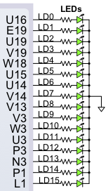
    module TOP(
        input clock,
        input reset,
        output [15:0] LED
        );

    reg [28:0] counter;
    always @ (posedge clock)
        if (reset) counter <= 0;
        else counter <= counter + 1;

    assign LED = counter[28:13];

    endmodule
We've added a "reset" line, and we can deside later how to assign this to
something on the board, like one of the push buttons (having a reset line
makes simulation easier). The counter is defined using the "reg" type,
the reset is synchronous with the clock, and the counter counts up. When it
gets to all 1's, it will turn over, which is perfectly fine for these
purposes. To blink the LEDs, we use the "assign" statement, and tie the
LED lines to the upper 16 bits of the counter. The statement
" assign LED = counter[28:13];" is understood by Verilog to mean ALL of the
LED bits (since we did not specify them), and will throw an error if the
number of bits in LED doesn't match the number of bits in counter.
    set_property PACKAGE_PIN W5 [get_ports clock]
    set_property IOSTANDARD LVCMOS33 [get_ports clock]
The first line ties pin "W5" to the port "clock", and the 2nd line sets the
IO "standard" to LVCMOS33, which means low voltage CMOS at 3.3 volts. That
means that the clock signal will toggle below 3.3V and above 3.3V to
differentiate 0 from 1. This is the usual standard for this chip (there
are others, more on that some other time).
## clock
set_property PACKAGE_PIN W5 [get_ports clock]
set_property IOSTANDARD LVCMOS33 [get_ports clock]
##
## reset
set_property PACKAGE_PIN T18 [get_ports reset]
set_property IOSTANDARD LVCMOS33 [get_ports reset]
##
## 16 LEDs
set_property PACKAGE_PIN L1 [get_ports {LED[15]}]
set_property IOSTANDARD LVCMOS33 [get_ports {LED[15]}]
set_property PACKAGE_PIN P1 [get_ports {LED[14]}]
set_property IOSTANDARD LVCMOS33 [get_ports {LED[14]}]
set_property PACKAGE_PIN N3 [get_ports {LED[13]}]
set_property IOSTANDARD LVCMOS33 [get_ports {LED[13]}]
set_property PACKAGE_PIN P3 [get_ports {LED[12]}]
set_property IOSTANDARD LVCMOS33 [get_ports {LED[12]}]
set_property PACKAGE_PIN U3 [get_ports {LED[11]}]
set_property IOSTANDARD LVCMOS33 [get_ports {LED[11]}]
set_property PACKAGE_PIN W3 [get_ports {LED[10]}]
set_property IOSTANDARD LVCMOS33 [get_ports {LED[10]}]
set_property PACKAGE_PIN V3 [get_ports {LED[9]}]
set_property IOSTANDARD LVCMOS33 [get_ports {LED[9]}]
set_property PACKAGE_PIN V13 [get_ports {LED[8]}]
set_property IOSTANDARD LVCMOS33 [get_ports {LED[8]}]
set_property PACKAGE_PIN V14 [get_ports {LED[7]}]
set_property IOSTANDARD LVCMOS33 [get_ports {LED[7]}]
set_property PACKAGE_PIN U14 [get_ports {LED[6]}]
set_property IOSTANDARD LVCMOS33 [get_ports {LED[6]}]
set_property PACKAGE_PIN U15 [get_ports {LED[5]}]
set_property IOSTANDARD LVCMOS33 [get_ports {LED[5]}]
set_property PACKAGE_PIN W18 [get_ports {LED[4]}]
set_property IOSTANDARD LVCMOS33 [get_ports {LED[4]}]
set_property PACKAGE_PIN V19 [get_ports {LED[3]}]
set_property IOSTANDARD LVCMOS33 [get_ports {LED[3]}]
set_property PACKAGE_PIN U19 [get_ports {LED[2]}]
set_property IOSTANDARD LVCMOS33 [get_ports {LED[2]}]
set_property PACKAGE_PIN E19 [get_ports {LED[1]}]
set_property IOSTANDARD LVCMOS33 [get_ports {LED[1]}]
set_property PACKAGE_PIN U16 [get_ports {LED[0]}]
set_property IOSTANDARD LVCMOS33 [get_ports {LED[0]}]
Save these changes. The program should look something like this:

Counter with Display
##
## buttons
set_property IOSTANDARD LVCMOS33 [get_ports reset]
set_property PACKAGE_PIN U17 [get_ports reset]
set_property IOSTANDARD LVCMOS33 [get_ports btnCnt]
set_property PACKAGE_PIN U18 [get_ports btnCnt]
The LEDs will be the same as above. The LED display works in the
following way: Each digit has an enable, and 8 inputs corresdponding
to each of the 8 LED parts as in the figure below:
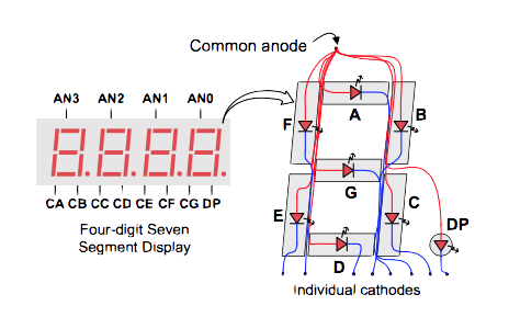
## clock
set_property PACKAGE_PIN W5 [get_ports clk]
set_property IOSTANDARD LVCMOS33 [get_ports clk]
##
## 16 LEDs
set_property PACKAGE_PIN L1 [get_ports {LED[15]}]
set_property IOSTANDARD LVCMOS33 [get_ports {LED[15]}]
set_property PACKAGE_PIN P1 [get_ports {LED[14]}]
set_property IOSTANDARD LVCMOS33 [get_ports {LED[14]}]
set_property PACKAGE_PIN N3 [get_ports {LED[13]}]
set_property IOSTANDARD LVCMOS33 [get_ports {LED[13]}]
set_property PACKAGE_PIN P3 [get_ports {LED[12]}]
set_property IOSTANDARD LVCMOS33 [get_ports {LED[12]}]
set_property PACKAGE_PIN U3 [get_ports {LED[11]}]
set_property IOSTANDARD LVCMOS33 [get_ports {LED[11]}]
set_property PACKAGE_PIN W3 [get_ports {LED[10]}]
set_property IOSTANDARD LVCMOS33 [get_ports {LED[10]}]
set_property PACKAGE_PIN V3 [get_ports {LED[9]}]
set_property IOSTANDARD LVCMOS33 [get_ports {LED[9]}]
set_property PACKAGE_PIN V13 [get_ports {LED[8]}]
set_property IOSTANDARD LVCMOS33 [get_ports {LED[8]}]
set_property PACKAGE_PIN V14 [get_ports {LED[7]}]
set_property IOSTANDARD LVCMOS33 [get_ports {LED[7]}]
set_property PACKAGE_PIN U14 [get_ports {LED[6]}]
set_property IOSTANDARD LVCMOS33 [get_ports {LED[6]}]
set_property PACKAGE_PIN U15 [get_ports {LED[5]}]
set_property IOSTANDARD LVCMOS33 [get_ports {LED[5]}]
set_property PACKAGE_PIN W18 [get_ports {LED[4]}]
set_property IOSTANDARD LVCMOS33 [get_ports {LED[4]}]
set_property PACKAGE_PIN V19 [get_ports {LED[3]}]
set_property IOSTANDARD LVCMOS33 [get_ports {LED[3]}]
set_property PACKAGE_PIN U19 [get_ports {LED[2]}]
set_property IOSTANDARD LVCMOS33 [get_ports {LED[2]}]
set_property PACKAGE_PIN E19 [get_ports {LED[1]}]
set_property IOSTANDARD LVCMOS33 [get_ports {LED[1]}]
set_property PACKAGE_PIN U16 [get_ports {LED[0]}]
set_property IOSTANDARD LVCMOS33 [get_ports {LED[0]}]
##
## buttons
set_property PACKAGE_PIN T18 [get_ports reset]
set_property IOSTANDARD LVCMOS33 [get_ports reset]
set_property PACKAGE_PIN U17 [get_ports btnCnt]
set_property IOSTANDARD LVCMOS33 [get_ports btnCnt]
##
## 7 segment display
set_property PACKAGE_PIN W7 [get_ports {segment[0]} ]
set_property IOSTANDARD LVCMOS33 [get_ports {segment[0]} ]
set_property PACKAGE_PIN W6 [get_ports {segment[1]} ]
set_property IOSTANDARD LVCMOS33 [get_ports {segment[1]} ]
set_property PACKAGE_PIN U8 [get_ports {segment[2]} ]
set_property IOSTANDARD LVCMOS33 [get_ports {segment[2]} ]
set_property PACKAGE_PIN V8 [get_ports {segment[3]} ]
set_property IOSTANDARD LVCMOS33 [get_ports {segment[3]} ]
set_property PACKAGE_PIN U5 [get_ports {segment[4]} ]
set_property IOSTANDARD LVCMOS33 [get_ports {segment[4]} ]
set_property PACKAGE_PIN V5 [get_ports {segment[5]} ]
set_property IOSTANDARD LVCMOS33 [get_ports {segment[5]} ]
set_property PACKAGE_PIN U7 [get_ports {segment[6]} ]
set_property IOSTANDARD LVCMOS33 [get_ports {segment[6]} ]
##
## LED period (dot)
set_property PACKAGE_PIN V7 [get_ports dp]
set_property IOSTANDARD LVCMOS33 [get_ports dp]
##
## digit select
set_property PACKAGE_PIN U2 [get_ports digit[0] ]
set_property IOSTANDARD LVCMOS33 [get_ports digit[0] ]
set_property PACKAGE_PIN U4 [get_ports {digit[1]} ]
set_property IOSTANDARD LVCMOS33 [get_ports {digit[1]} ]
set_property PACKAGE_PIN V4 [get_ports {digit[2]} ]
set_property IOSTANDARD LVCMOS33 [get_ports {digit[2]} ]
set_property PACKAGE_PIN W4 [get_ports {digit[3]} ]
set_property IOSTANDARD LVCMOS33 [get_ports {digit[3]} ]
    module TOP (
        input clk, reset, btnCnt,
        output [15:0] LED,
        output [6:0] segment,
        output dp,
        output [3:0] digit
    );
The way the display works is a little tricky. The diagram above shows
you what LEDs to turn on in order to get a certain number to be
displayed. By turning on one of the LED segments, you cause
current to flow through that segment. However, the current only
flows if the corresponding select bit (digit[3:0]) is set, as in the
following diagram:
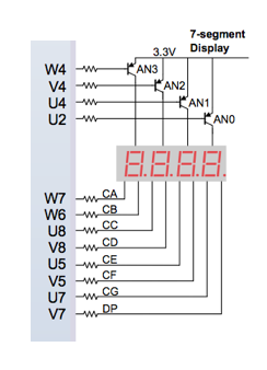
`timescale 1ns / 1ps
//////////////////////////////////////////////////////////////////////////////////
// Company:
// Engineer:
//
// Create Date: 08/15/2017 02:34:58 PM
// Design Name:
// Module Name: segnum
// Project Name:
// Target Devices:
// Tool Versions:
// Description:
//
// Dependencies:
//
// Revision:
// Revision 0.01 - File Created
// Additional Comments:
//
//////////////////////////////////////////////////////////////////////////////////
`timescale 1ns / 1ps

module segnum (
    input clk,
    input [3:0] number,
    output reg [6:0] seg = 0
    );

    parameter [6:0] p0 = 'b1000000;
    parameter [6:0] p1 = 'b1111001;
    parameter [6:0] p2 = 'b0100100;
    parameter [6:0] p3 = 'b0110000;
    parameter [6:0] p4 = 'b0011001;
    parameter [6:0] p5 = 'b0010010;
    parameter [6:0] p6 = 'b0000010;
    parameter [6:0] p7 = 'b1111000;
    parameter [6:0] p8 = 'b0000000;
    parameter [6:0] p9 = 'b0010000;
    parameter [6:0] pa = 'b0001000;
    parameter [6:0] pb = 'b0000011;
    parameter [6:0] pc = 'b1000110;
    parameter [6:0] pd = 'b0100001;
    parameter [6:0] pe = 'b0000110;
    parameter [6:0] pf = 'b0001110;
    parameter [6:0] pp = 'b1111101;

    always @ (posedge clk)
        case (number)
            'h0: seg <= p0;
            'h1: seg <= p1;
            'h2: seg <= p2;
            'h3: seg <= p3;
            'h4: seg <= p4;
            'h5: seg <= p5;
            'h6: seg <= p6;
            'h7: seg <= p7;
            'h8: seg <= p8;
            'h9: seg <= p9;
            'hA: seg <= pa;
            'hB: seg <= pb;
            'hC: seg <= pc;
            'hD: seg <= pd;
            'hE: seg <= pe;
            'hF: seg <= pf;
            default: seg <= pp;
        endcase


endmodule
module display4(
    input clk100,
    output reg [3:0] digit = 0,  //digit 3 is leftmost (MSD), digit 1 is rightmost (LSD)
    output reg [6:0] segments = 'b111111, //7 segments: top,mid,bot and top_left/bot_left and same for right
    output reg period,
    input [15:0] number     //4 hex digits
    );
We associate the 4-bit digit with the 16-bit number like this:
wire [3:0] digit3 = number[15:12];
wire [3:0] digit2 = number[11:8];
wire [3:0] digit1 = number[7:4];
wire [3:0] digit0 = number[3:0];
Next we make a clock from the 100MHz input clock that will refresh
at a high enough rate so that there's no flickering. 60Hz means
a 16ms period. If we start with a 10ns period, then we need around
$10^6$ ticks of the 100MHz clock for each refresh, which means a
counter that's around 20 bits. So we can make a 19 bit counter
and use the MSB, and that will be at least 16ms (it will be around
5ms, which means more like 200Hz refresh will be just fine). However,
due to the fact that we can only send 1 of 4 digits at a time, and
we have to cycle through, we need to run this slower clock 4x faster.
So we will make an 18-bit counter, and use bit 17 (starting from 0)
as the clock, and increment a 2-bit register for the digit pointer.
The code will look something like this:
reg [17:0] counter = 0;
always @ (posedge clk100) counter <= counter + 1;
wire digit_clock = counter[17];
reg [1:0] which_digit;
always @ (posedge digit_clock) which_digit <= which_digit + 1;
Putting it all together, we make a case statement inside an
always block using digit_clock as the posedge trigger, use
segnum to set the segment display, and loop. The full code for
display4.v looks like this:
`timescale 1ns / 1ps
//////////////////////////////////////////////////////////////////////////////////
// Company:
// Engineer:
//
// Create Date: 08/14/2017 04:14:07 PM
// Design Name:
// Module Name: counter
// Project Name:
// Target Devices:
// Tool Versions:
// Description:
//
// Dependencies:
//
// Revision:
// Revision 0.01 - File Created
// Additional Comments:
//
//////////////////////////////////////////////////////////////////////////////////
`timescale 1ns / 1ps


module display4(
    input clk100,
    output reg [3:0] digit = 0,  //digit 3 is leftmost (MSD), digit 1 is rightmost (LSD)
    output reg [6:0] segments = 'b111111, //7 segments: top,mid,bot and top_left/bot_left and same for right
    output reg period,
    input [15:0] number     //4 hex digits
    );


//
// well, verilog arithmetic is pretty good so let's just let it figure out the digits
//
wire [3:0] digit3 = number[15:12];
wire [3:0] digit2 = number[11:8];
wire [3:0] digit1 = number[7:4];
wire [3:0] digit0 = number[3:0];

//
// make a clock from the 100MHz clock that refreshes at around 60Hz or more.
// that means a period of at least 16ms.   with a 10ns period input clock,
// if you set up a register with N bits, the period is given by:
// T = 10ns * 2^{N+1}
// so we want 16ms = 10ns * 2^{N+1} solving for that gives 19.6 bits so we use 19
// to make it a little faster than 60Hz.
//
// But, since we can only have one digit on at a time, we need to change the digits
// by 4 times this value.   that means we need to run the clock 4x faster, and use
// that slow clock to increment a 2-bit pointer and cycle through the 4 digits one at a time
//
reg [17:0] counter = 0;
//
// use negedge so we don't have race conditions later
//
always @ (negedge clk100) counter <= counter + 1;
wire digit_clock = counter[17];
reg [1:0] which_digit;
always @ (posedge digit_clock) which_digit <= which_digit + 1;

wire [6:0] wseg0, wseg1, wseg2, wseg3;
segnum S0 ( .clk(clk100), .number(digit0), .seg(wseg0) );
segnum S1 ( .clk(clk100), .number(digit1), .seg(wseg1) );
segnum S2 ( .clk(clk100), .number(digit2), .seg(wseg2) );
segnum S3 ( .clk(clk100), .number(digit3), .seg(wseg3) );

always @ (posedge digit_clock) begin
    period <= 1;       // turn it off for now
    case (which_digit)
        'h0: begin
                digit <= 'b1110;
                segments <= wseg0;
            end
        'h1: begin
                digit <= 'b1101;
                segments <= wseg1;
            end
        'h2: begin
                digit <= 'b1011;
                segments <= wseg2;
            end
        'h3: begin
                digit <= 'b0111;
                segments <= wseg3;
            end
      endcase
end

endmodule
Before putting this together, we first need to consider the push button
counter action. Pushing buttons is notoriously dangerous because of
"bouncing".
The basys3 board contains some RC components on the push buttons, and
that will filter out the high frequency bouncing, but if your finger
bounces (too much coffee?) then it won't filter that out.
If you simply register an input (e.g. the push button
input) with the 100MHz system clock, you might count the bounces when
all you wanted to count was the single push.
So, there are many ways to "debounce", but one of the easiest
is to just make a new clock with a period long enough compared to
the bounces, and then latch the push button. What you should see is
the posedge of the clock, then the bounces, then it will settle down,
then more posedges. If you then trigger on the posedge of the registered
signal, you should only see a single edge there, and that is the signal
you count. The diagram below illustrates the "Push", the clock, and
the "Trigger".
   //
    // look at the counter input (btnCnt).  use that to make a 1-shot
    // use a longer period clock than 10ns for the 1-shot just to get rid
    // of "bouncing"
    //
    reg [14:0] clock_count;
    always @ (posedge clk)
        if (reset) clock_count <= 0;
        else clock_count <= clock_count + 1;
    reg [15:0] the_count;
    wire slow_clk = clock_count[14];
    reg trigger;
    always @ (posedge slow_clk) trigger <= btnCnt;
    //
    // now count "triggers"
    always @ (posedge trigger or posedge reset)
        if (reset) the_count <= 0;
        else the_count <= the_count + 1;
One more thing - this code will count and display a hex number in the
LED display.
We can change it easily so that it displays decimal, by counting, and
incrementing each digit when the previous digit is 9 (decimal).
You have to be careful about this, because it will happen inside an
always block, which means everything happens on 1 clock tick!
Let's look at some code snippets to do this.
    reg [15:0] the_count;
    reg [3:0] the_count_d0;
    reg [3:0] the_count_d1;
    reg [3:0] the_count_d2;
    reg [3:0] the_count_d3;
    wire [15:0] count_d = {the_count_d3,the_count_d2,the_count_d1,the_count_d0};=
You can see also that we define a 16-digit wire made up of the
concatenation of the 4 digits (concatenations are always inside {} pairs).
So the bus "count_d" will contain the 4 digits, and the lower order digit
(the 1s digit) will be the_count_d0. The bus "count_d" will be sent into
display4.v instead of "the_count".
    if ( the_count_d0 == 'h9 ) begin
        the_count_d0 <= 0;
        if ( the_count_d1 == 'h9 ) begin
            the_count_d1 <= 0;
            if ( the_count_d2 == 'h9 ) begin
                the_count_d2 <= 0;
                if ( the_count_d3 == 'h9 ) the_count_d3 <= 0;
                else the_count_d3 <= the_count_d3 + 1;
            end
            else the_count_d2 <= the_count_d2 + 1;
        end
        else the_count_d1 <= the_count_d1 + 1;
    end
    else the_count_d0 <= the_count_d0 + 1;
So, what you do is to check the 1st digit ("the_count_d0"), and if it's
already 9, then set it to 0 and check the 10s digit. If that's already
9, then set it to 0 and check the 100s. And so on.
`timescale 1ns / 1ps
//////////////////////////////////////////////////////////////////////////////////
// Company:
// Engineer:
//
// Create Date: 10/05/2017 01:36:42 PM
// Design Name:
// Module Name: TOP
// Project Name:
// Target Devices:
// Tool Versions:
// Description:
//
// Dependencies:
//
// Revision:
// Revision 0.01 - File Created
// Additional Comments:
//
//////////////////////////////////////////////////////////////////////////////////


module TOP(
    input clk,
    input reset, btnCnt,
    output [15:0] LED,
    output [6:0] segment,
    output dp,
    output [3:0] digit
    );

    //
    // look at the counter input (btnCnt).  use that to make a 1-shot
    // use a longer period clock than 10ns for the 1-shot just to get rid
    // of "bouncing"
    //
    reg [19:0] clock_count;
    always @ (posedge clk)
        if (reset) clock_count <= 0;
        else clock_count <= clock_count + 1;
    reg [15:0] the_count;
    reg [3:0] the_count_d0;
    reg [3:0] the_count_d1;
    reg [3:0] the_count_d2;
    reg [3:0] the_count_d3;
    wire [15:0] count_d = {the_count_d3,the_count_d2,the_count_d1,the_count_d0};
    wire slow_clk = clock_count[14];
    reg trigger;
    always @ (posedge slow_clk) trigger <= btnCnt;
    //
    // now count "triggers"
    always @ (posedge trigger or posedge reset)
        if (reset) begin
            the_count <= 0;
            the_count_d0 <= 0;
            the_count_d1 <= 0;
            the_count_d2 <= 0;
            the_count_d3 <= 0;
            end
        else begin
            //
            // check each digit of the_count decimal parts
            //
            if ( the_count_d0 == 'h9 ) begin
                the_count_d0 <= 0;
                if ( the_count_d1 == 'h9 ) begin
                    the_count_d1 <= 0;
                    if ( the_count_d2 == 'h9 ) begin
                        the_count_d2 <= 0;
                        if ( the_count_d3 == 'h9 ) the_count_d3 <= 0;
                        else the_count_d3 <= the_count_d3 + 1;
                    end
                    else the_count_d2 <= the_count_d2 + 1;
                end
                else the_count_d1 <= the_count_d1 + 1;
            end
            else the_count_d0 <= the_count_d0 + 1;

            the_count <= the_count + 1;
        end
    wire [3:0] which_digit;
    wire [6:0] dnumber;
    wire period;
    display4 DISPLAY (
        .clk100(clk),
        .digit(which_digit),
        .segments(dnumber),
        .period(period),
        .number(count_d));
//        .number(the_count));

    assign LED = the_count;
    assign dp = 1;
    assign segment = dnumber;
    assign digit = which_digit;

endmodule


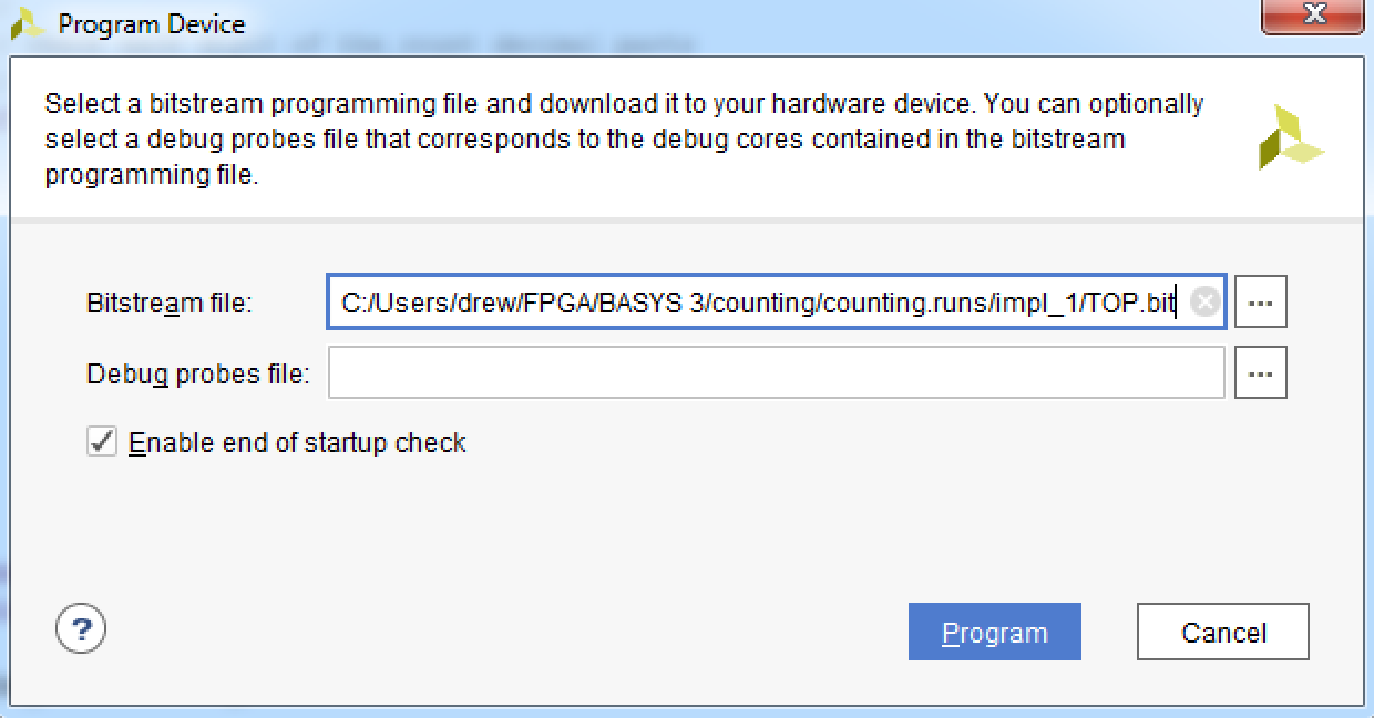
Programming Flash Ram

FPGA Computer Connection
Back to top
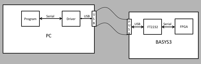
Talking to FPGAs over Serial Ports
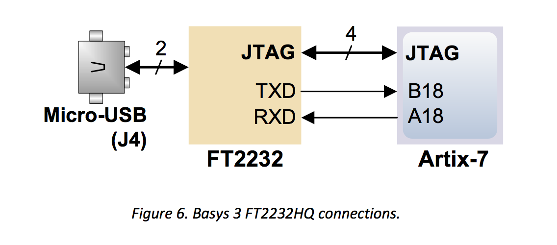
##USB-RS232 Interface
set_property PACKAGE_PIN B18 [get_ports RsRx]
set_property IOSTANDARD LVCMOS33 [get_ports RsRx]
set_property PACKAGE_PIN A18 [get_ports RsTx]
set_property IOSTANDARD LVCMOS33 [get_ports RsTx]

The timing diagram is shown below. Note that parity bits are optional, and the stop
bit can be 1, 1.5, or 2 bits wide. It's all up to the programmer, but of course the
transmitter and receiver have to agree.
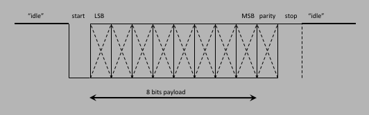
Serial Transmission
The verilog code for the RS232 serial transmitter can be found
here.
Usage is relatively simple. For the transmitter, you have the following ports:
   input        i_Clock,
   input [15:0] i_Clocks_per_Bit,
   input        i_Reset,
   input        i_Tx_DV,
   input [7:0]  i_Tx_Byte,
   output       o_Tx_Active,
   output reg   o_Tx_Serial,
   output       o_Tx_Done,
   output [7:0] o_debug
The i_Tx_DV line initiates the transfer. Outputs are:
    parameter CLKS_PER_BIT = 'd100;
    wire [15:0] clks_per_bit = CLKS_PER_BIT;
    wire [7:0] tdebug;
    wire tx_ready;
    wire [7:0] tx_data;
    wire tx_done;
    uart_tx (
        .i_Clock(clk),
        .i_Clocks_per_Bit(clks_per_bit),
        .i_Reset(reset),
        .i_Tx_DV(startit),
        .i_Tx_Byte(tx_data),
        .o_Tx_Serial(RsTx),
        .o_Tx_Active(tx_ready),
        .o_Tx_Done(tx_done),
        .o_debug(tdebug)
    );
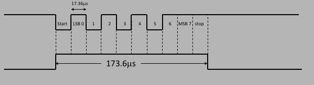
Serial Receiver
The verilog code for the RS232 serial receiver can be found
here.
Usage is also relatively simple. For the receiver, you have the following ports:
   input        i_Clock,
   input [15:0] i_Clocks_per_Bit,
   input        i_Reset,
   input        i_Rx_Serial,
   output       o_Rx_DV,
   output [7:0] o_Rx_Byte,
   output [7:0] o_debug
The i_Tx_DV line initiates the transfer. Outputs are:
Serial IO FPGA Code
`timescale 1ns / 1ps
//
// basic serial protocol IO device driver
//
// CLKS_BER_BIT = ratio of internal clock to baud rate desired
// o_debug: lower 7 bits come from RX, upper from TX module
//          see uart_* for what bits are where

module SerialIO #(parameter CLKS_PER_BIT = 'd100) (
    input i_Clock,
    input i_Reset,
    output o_Tx,
    input i_Rx,
    input i_Transmit,
    input [7:0] i_Tx_Byte,
    output o_Tx_Active,
    output o_Tx_Done,
    output [7:0] o_Rx_Byte,
    output o_Rx_DV,
    output o_debug

    );

//
// for now use the pb_down to trigger the tx
//
wire [15:0] clocks_per_bit = CLKS_PER_BIT;
wire [7:0] tdebug;
uart_tx TX (
    .i_Clocks_per_Bit(clocks_per_bit),
    .i_Clock(i_Clock),
    .i_Reset(i_Reset),
    .i_Tx_DV(i_Transmit),
    .i_Tx_Byte(i_Tx_Byte),
    .o_Tx_Serial(o_Tx),
    .o_Tx_Active(o_Tx_Active),
    .o_Tx_Done(o_Tx_Done),
    .o_debug(tdebug)
    );

wire [7:0] rdebug;
uart_rx RX  (
    .i_Clocks_per_Bit(clocks_per_bit),
    .i_Clock(i_Clock),
    .i_Reset(i_Reset),
    .i_Rx_Serial(i_Rx),
    .o_Rx_Byte(o_Rx_Byte),
    .o_Rx_DV(o_Rx_DV),
    .o_debug(rdebug)
    );

assign o_debug = {tdebug,rdebug};

endmodule
    .
    .
    .
    wire rx_dv;
    wire [7:0] rx_data;
    wire [15:0] debugit;
    wire tx_ready;
    wire [7:0] tx_data = sw;
    wire tx_done;
    SerialIO  # (.CLKS_PER_BIT(CLOCK_DIVIDER)) serial (
        .i_Clock(clk),
        .i_Reset(reset),
        // transmitter:
        .o_Tx(RsTx),
        .i_Transmit(pb_down),
        .i_Tx_Byte(tx_data),
        .o_Tx_Active(tx_ready),
        .o_Tx_Done(tx_done),
        // receiver:
        .i_Rx(RsRx),
        .o_Rx_Byte(rx_data),
        .o_Rx_DV(rx_dv),
        // debug, can change to .o_debug() if not needed
        .o_debug(debugit)
    );
    .
    .
    .
Here you see a new bit of syntax in the instantiation:
module #(.parameter(value)) instantiation (...);
The hash tag # is used to designate a list of parameters, and their values.
Here we use the parameter "CLKS_PER_BIT", which corresponds to the name of the
parameter in the SerialIO module, and "CLOCK_DIVIDER", which we set in the
top level code
in the following way:
parameter CLOCK_DIVIDER = 'd100; // 1MHz baud
BASYS3 Serial IO Example (USB_Serial1)
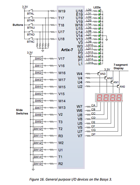
## Switches
set_property PACKAGE_PIN V17 [get_ports {sw[0]}]
set_property IOSTANDARD LVCMOS33 [get_ports {sw[0]}]
set_property PACKAGE_PIN V16 [get_ports {sw[1]}]
set_property IOSTANDARD LVCMOS33 [get_ports {sw[1]}]
set_property PACKAGE_PIN W16 [get_ports {sw[2]}]
set_property IOSTANDARD LVCMOS33 [get_ports {sw[2]}]
set_property PACKAGE_PIN W17 [get_ports {sw[3]}]
set_property IOSTANDARD LVCMOS33 [get_ports {sw[3]}]
set_property PACKAGE_PIN W15 [get_ports {sw[4]}]
set_property IOSTANDARD LVCMOS33 [get_ports {sw[4]}]
set_property PACKAGE_PIN V15 [get_ports {sw[5]}]
set_property IOSTANDARD LVCMOS33 [get_ports {sw[5]}]
set_property PACKAGE_PIN W14 [get_ports {sw[6]}]
set_property IOSTANDARD LVCMOS33 [get_ports {sw[6]}]
set_property PACKAGE_PIN W13 [get_ports {sw[7]}]
set_property IOSTANDARD LVCMOS33 [get_ports {sw[7]}]

# LEDs
set_property PACKAGE_PIN U16 [get_ports {led[0]}]
set_property IOSTANDARD LVCMOS33 [get_ports {led[0]}]
set_property PACKAGE_PIN E19 [get_ports {led[1]}]
set_property IOSTANDARD LVCMOS33 [get_ports {led[1]}]
set_property PACKAGE_PIN U19 [get_ports {led[2]}]
set_property IOSTANDARD LVCMOS33 [get_ports {led[2]}]
set_property PACKAGE_PIN V19 [get_ports {led[3]}]
set_property IOSTANDARD LVCMOS33 [get_ports {led[3]}]
set_property PACKAGE_PIN W18 [get_ports {led[4]}]
set_property IOSTANDARD LVCMOS33 [get_ports {led[4]}]
set_property PACKAGE_PIN U15 [get_ports {led[5]}]
set_property IOSTANDARD LVCMOS33 [get_ports {led[5]}]
set_property PACKAGE_PIN U14 [get_ports {led[6]}]
set_property IOSTANDARD LVCMOS33 [get_ports {led[6]}]
set_property PACKAGE_PIN V14 [get_ports {led[7]}]
set_property IOSTANDARD LVCMOS33 [get_ports {led[7]}]
set_property PACKAGE_PIN V13 [get_ports {led[8]}]
set_property IOSTANDARD LVCMOS33 [get_ports {led[8]}]
set_property PACKAGE_PIN V3 [get_ports {led[9]}]
set_property IOSTANDARD LVCMOS33 [get_ports {led[9]}]
set_property PACKAGE_PIN W3 [get_ports {led[10]}]
set_property IOSTANDARD LVCMOS33 [get_ports {led[10]}]
set_property PACKAGE_PIN U3 [get_ports {led[11]}]
set_property IOSTANDARD LVCMOS33 [get_ports {led[11]}]
set_property PACKAGE_PIN P3 [get_ports {led[12]}]
set_property IOSTANDARD LVCMOS33 [get_ports {led[12]}]
set_property PACKAGE_PIN N3 [get_ports {led[13]}]
set_property IOSTANDARD LVCMOS33 [get_ports {led[13]}]
set_property PACKAGE_PIN P1 [get_ports {led[14]}]
set_property IOSTANDARD LVCMOS33 [get_ports {led[14]}]
set_property PACKAGE_PIN L1 [get_ports {led[15]}]
set_property IOSTANDARD LVCMOS33 [get_ports {led[15]}]
From the above, you can then set these inputs and outputs in
your toplevel by doing the following:
    input [7:0] sw,
    output [15:0] led,
    .
    .
    .
    wire rx_dv;
    wire [7:0] rx_data;
    wire [15:0] debugit;
    wire tx_ready;
    wire [7:0] tx_data = sw;
    wire tx_done;
    SerialIO  # (.CLKS_PER_BIT(CLOCK_DIVIDER)) serial (
        .i_Clock(clk),
        .i_Reset(reset),
        // transmitter:
        .o_Tx(RsTx),
        .i_Transmit(pb_down),
        .i_Tx_Byte(tx_data),
        .o_Tx_Active(tx_ready),
        .o_Tx_Done(tx_done),
        // receiver:
        .i_Rx(RsRx),
        .o_Rx_Byte(rx_data),
        .o_Rx_DV(rx_dv),
        // debug, can change to .o_debug() if not needed
        .o_debug(debugit)
    );
    assign led[12] = ~tx_ready;
    assign led[7:0] = rx_data;
    .
    .
    .
    module PB_Debouncer(
        // inputs
        input i_clk,
        input i_reset,
        input i_PB,  // "PB" is the glitchy, asynchronous to clk, active low push-button signal
        // outputs: we make three outputs, all synchronous to the clock
        output reg o_PB_state,  // 1 as long as the push-button is active (down)
        output reg o_PB_down,  // 1 for one clock cycle when the push-button goes down (i.e. just pushed)
        output reg o_PB_up,   // 1 for one clock cycle when the push-button goes up (i.e. just released)
        output [7:0] o_debug   // for debugging, optional
);
Connecting to a PC
![]()
Data
Back to top
Digital IO

##Pmod Header JA
##Sch name = JA1
set_property PACKAGE_PIN J1 [get_ports {JA[0]}]
set_property IOSTANDARD LVCMOS33 [get_ports {JA[0]}]
##Sch name = JA2
set_property PACKAGE_PIN L2 [get_ports {JA[1]}]
set_property IOSTANDARD LVCMOS33 [get_ports {JA[1]}]
##Sch name = JA3
set_property PACKAGE_PIN J2 [get_ports {JA[2]}]
set_property IOSTANDARD LVCMOS33 [get_ports {JA[2]}]
##Sch name = JA4
set_property PACKAGE_PIN G2 [get_ports {JA[3]}]
set_property IOSTANDARD LVCMOS33 [get_ports {JA[3]}]
##Sch name = JA7
set_property PACKAGE_PIN H1 [get_ports {JA[4]}]
set_property IOSTANDARD LVCMOS33 [get_ports {JA[4]}]
##Sch name = JA8
set_property PACKAGE_PIN K2 [get_ports {JA[5]}]
set_property IOSTANDARD LVCMOS33 [get_ports {JA[5]}]
##Sch name = JA9
set_property PACKAGE_PIN H2 [get_ports {JA[6]}]
set_property IOSTANDARD LVCMOS33 [get_ports {JA[6]}]
##Sch name = JA10
set_property PACKAGE_PIN G3 [get_ports {JA[7]}]
set_property IOSTANDARD LVCMOS33 [get_ports {JA[7]}]
    .
    .
    .
    input [7:0] JA,
    .
    .
    .
The .xdc file specifies the i/o standard as "LVCMOS33",
which just means that it expects the signal to go between
0 volts (digital 0) and 3.3 volts (digital 1). Other
standards are of course possible.
LVDS Input
J1 IO_L3N_T0_DQS_AD5N_35 ....
set_property PACKAGE_PIN H1 [get_ports lvds1_p ]
set_property IOSTANDARD LVDS_25 [get_ports lvds1_p ]
set_property PACKAGE_PIN J1 [get_ports lvds1_n ]
set_property IOSTANDARD LVDS_25 [get_ports lvds1_n ]
    module .... (
        .
        .
        .
        input lvds1_p, lvds1_n,   // Pmod JA, 1 (J1) and 7 (H1) right most pair top and bottom of connector
        .
        .
        .
    );
    .
    .
    .
    wire single_ended;
    IBUFDS dif2single1 (.I(lvds1_p), .IB(lvds1_n), .O(single_ended) );
    .
    .
    .
The IBUFDS instantiation is an internal Xilinx "primitive" that they
provide, so all you have to do is refer to it correctly. It will take
the 2 differential inputs and turn them into a single ended signal that
you can use.
Analog IO
CPG236 Name Artix7 pin BASYS3 JXADC Pin
IO_L7P_T1_AD6P_35 J3 1
IO_L7N_T1_AD6N_35 K3 7
IO_L8P_T1_AD14P_35 L3 2
IO_L8N_T1_AD14N_35 M3 8
IO_L9P_T1_DQS_AD7P_35 M2 3
IO_L9N_T1_DQS_AD7N_35 M1 9
IO_L10P_T1_AD15P_35 N2 4
IO_L10N_T1_AD15N_35 N1 10
Xilinx XADC
Xilinx XADC Timing
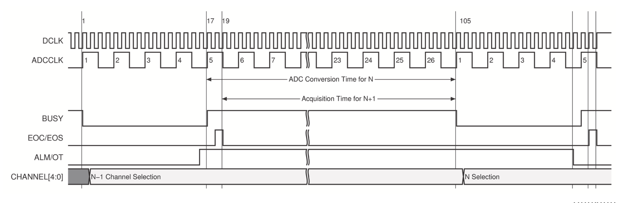
XADC Instantiation Using IP Wizard

Now you are ready to generate the instantiation. You will see in the
left panel what pins will be driven, it should look like this:
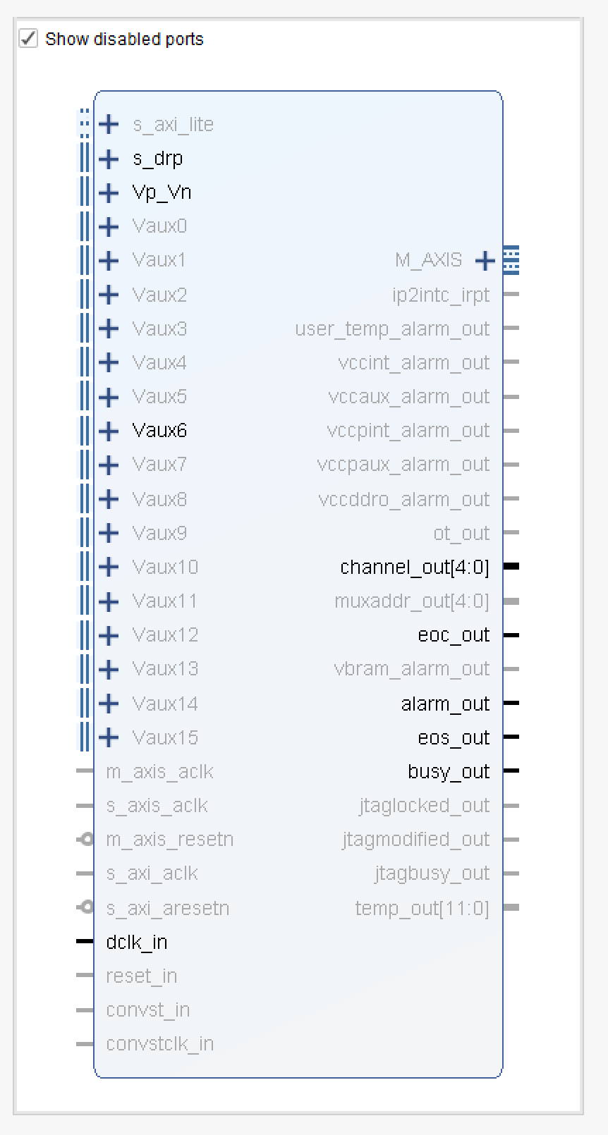
    xadc_wiz_0 XADC_INST (
        .daddr_in(daddr_in[6:0]),
        .dclk_in(dclk_in),
        .den_in(den_in),
        .di_in(di_in[15:0]),
        .dwe_in(dwe_in),
        .vauxp6(vauxp6),
        .vauxn6(vauxn6),
        .busy_out(busy_out),
        .channel_out(channel_out[4:0]),
        .do_out(do_out[15:0]),
        .drdy_out(drdy_out),
        .eoc_out(eoc_out),
        .eos_out(eos_out),
        .alarm_out(alarm_out),
        .vp_in(vp_in),
        .vn_in(vn_in)
    );
Here's what you do with each of these ports:
        .INIT_40(16'h0016), // config reg 0
        .INIT_41(16'h31AF), // config reg 1
        .INIT_42(16'h0200), // config reg 2
        .INIT_48(16'h0100), // Sequencer channel selection
        .INIT_49(16'h0000), // Sequencer channel selection
        .INIT_4A(16'h0000), // Sequencer Average selection
        .INIT_4B(16'h0000), // Sequencer Average selection
        .INIT_4C(16'h0000), // Sequencer Bipolar selection
        .INIT_4D(16'h0000), // Sequencer Bipolar selection
        .INIT_4E(16'h0000), // Sequencer Acq time selection
        .INIT_4F(16'h0000), // Sequencer Acq time selection
        .INIT_50(16'hB5ED), // Temp alarm trigger
        .INIT_51(16'h57E4), // Vccint upper alarm limit
        .INIT_52(16'hA147), // Vccaux upper alarm limit
        .INIT_53(16'hCA33),  // Temp alarm OT upper
        .INIT_54(16'hA93A), // Temp alarm reset
        .INIT_55(16'h52C6), // Vccint lower alarm limit
        .INIT_56(16'h9555), // Vccaux lower alarm limit
        .INIT_57(16'hAE4E),  // Temp alarm OT reset
        .INIT_58(16'h5999), // VCCBRAM upper alarm limit
        .INIT_5C(16'h5111),  //  VCCBRAM lower alarm limit
The following table summarizes the configuration registers. For our purposes, since we are running in continuous single channel mode and no alarms, only the configuration registers are important.
Register (hex) Value
Name Comments
40 'h0016 config reg 0
4:0 selects ADC input channels, 16 means VAUX 6 only.
Settling time is 4 ticks, continuous mode,
unipolar, no external multiplexer mode,
and use averaging to calculate calibration coefficients.
41 'h31AF config reg 1
disable temperature alarms, enable ADC gain corrections, disable offset
corrections, set single channel mode
42 'h0200 config reg 2
ADCCLK = dclk_in divided by x2
FPGA Voltmeter
Back to top
    module top(
        input clk,
        input btnC,         // for serial IO start
        input btnL,         // for triggering ADC latching
        input btnU,         // to display version number on LED display
        input btnR,         // for reset
        output RsTx,        // uart Transmit
        input RsRx,         // uart Receive
        input adc_n, adc_p, // VCAUX 6, P and N
        output [15:0] led,  // 16 onboard LEDs above the switches
        output [6:0] segment,   // 4 digit LED display
        output dp,              // "." next to each LED digit
        output [3:0] digit,     // specifies which digit to display
        output [7:0] JA,        // headers for looking at signals on logic analyzers
        output [7:0] JB,
        output [7:0] JC
    );
The figure below shows explicitly how the buttons are labeled:
    parameter CLOCK_DIVIDER = 'd100;  // 100MHz/1Mbaud
    parameter VERSION = 'h2001;
CLOCK_DIVIDER is for the serial transmission baud rate, and VERSION
can be anything you want
    //
    // CLOCK SECTION HERE....  clock = 327us and clk20 = 20ns
    //
    wire clock2, clk2;
    ClkSynth synth (.clock_in(clk), .clock_slow(clock2), .clk20(clk2) );
    wire clock_slow, clk20;
    BUFG slowclk (.I(clock2),.O(clock_slow));
    BUFG clk20buf (.I(clk2),.O(clk20));
assign led = {~tx_ready,3'b000,r_adc_data};
We will use a state machine triggered by the push button btnL (debounced)
to latch the data from r_adc_data in a controlled an synchronized way.
The state machine
will start in the WAIT state, and when debounced btnL is asserted ("pbA_pushed"),
it will to into the "LATCH" state where it will latch the ADC value into a 12-bit
register called "latched_adc". It then goes into a "WAIT_END" state and
waits until the push button is released to go back again to WAIT, ready for the
next push button. At the end of the code you will see how the output
data headers "JA", "JB", and "JC" are defined, allowing one to look at these
signals with a logic analyzer.
    //
    // XADC instantiation
    //
    wire [6:0] daddr_in = 7'h16;
    wire adc_ready;
    wire eos_out, isbusy, alarm, adc_data_ready;
    wire [15:0] adc_data, data_in;
    assign data_in = 16'h0;
    wire [4:0] channel_out;
    reg [11:0] r_adc_data;
    localparam [1:0] WAIT=0, LATCH=1, WAIT_END=2;
    reg [1:0] adc_state;
    reg [11:0] latched_adc;
    //
    // wait for push button to digitize.  run FSM at 50MHz (mainly so we can see it on the Saleae!)
    //
    always @ (posedge clk20) begin
        if (reset) r_adc_data <= 12'h0;
        else if (adc_data_ready) r_adc_data <= adc_data[15:4];
        end
    //
    // FSM for latching adc value
    //
    always @ (posedge clk20) begin
        if (reset) begin
            adc_state <= WAIT;
            latched_adc <= 0;
        end
        case (adc_state)
            WAIT: begin
                //
                // watch for btnL or btnD to signal we want to latch something
                //
                if (pbL_pushed || pbD_pushed) adc_state <= LATCH;
                else adc_state <= WAIT;
            end
            LATCH: begin
                //
                // latch it
                //
                if (pbL_pushed) latched_adc <= r_adc_data;
                if (pbD_pushed) latched_adc <= {sw[7:0],4'h0};
                adc_state <= WAIT_END;
            end
            WAIT_END: begin
                //
                // wait for the button to no longer be pushed
                //
                if (pbL_pushed || pbD_pushed) adc_state <= WAIT_END;
                else adc_state <= WAIT;
            end
            default: begin
                adc_state <= WAIT;
            end
        endcase
    end
    //
    //  input clock is 50MHz (specify in the Wizard)
    //
    xadc_wiz_0 XADC_INST (
        .daddr_in(daddr_in),
        .dclk_in(clk20),
        .den_in(adc_ready),
        .di_in(data_in),
        .dwe_in(1'b0),
        .vauxp6(adc_p),
        .vauxn6(adc_n),
        .busy_out(isbusy),
        .channel_out(channel_out),
        .do_out(adc_data),
        .drdy_out(adc_data_ready),
        .eoc_out(adc_ready),
        .eos_out(eos_out),
        .alarm_out(alarm),
        .vp_in(1'b0),
        .vn_in(1'b0)
    );
    wire [7:0] tx_data = latched_adc[11:4];
    wire tx_done;
    SerialIO  # (.CLKS_PER_BIT(CLOCK_DIVIDER)) serial (
        .i_Clock(clk),
        .i_Reset(reset),
        // transmitter:
        .o_Tx(RsTx),
        .i_Transmit(pbC_down),
        .i_Tx_Byte(tx_data),
        .o_Tx_Active(tx_ready),
        .o_Tx_Done(tx_done),
        // receiver:
        .i_Rx(RsRx),
        .o_Rx_Byte(rx_data),
        .o_Rx_DV(rx_dv),
        .o_debug(debugit)
    );
    wire [15:0] display_this = pbU_pushed ? VERSION : {4'h0,latched_adc};
    display4 DISPLAY (
        .clk100(clk),
        .number(display_this),
        .digit(digit),
        .segments(segment),
        .period(dp)
        );
    assign JA = {r_adc_data[11:4]};
    assign JB = {clk20,adc_data_ready,adc_ready,isbusy,r_adc_data[3:0]};
    assign JC = {adc_data[15:8]};
## Switches
set_property PACKAGE_PIN V17 [get_ports {sw[0]}]
set_property IOSTANDARD LVCMOS33 [get_ports {sw[0]}]
set_property PACKAGE_PIN V16 [get_ports {sw[1]}]
set_property IOSTANDARD LVCMOS33 [get_ports {sw[1]}]
set_property PACKAGE_PIN W16 [get_ports {sw[2]}]
set_property IOSTANDARD LVCMOS33 [get_ports {sw[2]}]
set_property PACKAGE_PIN W17 [get_ports {sw[3]}]
set_property IOSTANDARD LVCMOS33 [get_ports {sw[3]}]
set_property PACKAGE_PIN W15 [get_ports {sw[4]}]
set_property IOSTANDARD LVCMOS33 [get_ports {sw[4]}]
set_property PACKAGE_PIN V15 [get_ports {sw[5]}]
set_property IOSTANDARD LVCMOS33 [get_ports {sw[5]}]
set_property PACKAGE_PIN W14 [get_ports {sw[6]}]
set_property IOSTANDARD LVCMOS33 [get_ports {sw[6]}]
set_property PACKAGE_PIN W13 [get_ports {sw[7]}]
set_property IOSTANDARD LVCMOS33 [get_ports {sw[7]}]
# LEDs
set_property PACKAGE_PIN U16 [get_ports {led[0]}]
set_property IOSTANDARD LVCMOS33 [get_ports {led[0]}]
set_property PACKAGE_PIN E19 [get_ports {led[1]}]
set_property IOSTANDARD LVCMOS33 [get_ports {led[1]}]
set_property PACKAGE_PIN U19 [get_ports {led[2]}]
set_property IOSTANDARD LVCMOS33 [get_ports {led[2]}]
set_property PACKAGE_PIN V19 [get_ports {led[3]}]
set_property IOSTANDARD LVCMOS33 [get_ports {led[3]}]
set_property PACKAGE_PIN W18 [get_ports {led[4]}]
set_property IOSTANDARD LVCMOS33 [get_ports {led[4]}]
set_property PACKAGE_PIN U15 [get_ports {led[5]}]
set_property IOSTANDARD LVCMOS33 [get_ports {led[5]}]
set_property PACKAGE_PIN U14 [get_ports {led[6]}]
set_property IOSTANDARD LVCMOS33 [get_ports {led[6]}]
set_property PACKAGE_PIN V14 [get_ports {led[7]}]
set_property IOSTANDARD LVCMOS33 [get_ports {led[7]}]
set_property PACKAGE_PIN V13 [get_ports {led[8]}]
set_property IOSTANDARD LVCMOS33 [get_ports {led[8]}]
set_property PACKAGE_PIN V3 [get_ports {led[9]}]
set_property IOSTANDARD LVCMOS33 [get_ports {led[9]}]
set_property PACKAGE_PIN W3 [get_ports {led[10]}]
set_property IOSTANDARD LVCMOS33 [get_ports {led[10]}]
set_property PACKAGE_PIN U3 [get_ports {led[11]}]
set_property IOSTANDARD LVCMOS33 [get_ports {led[11]}]
set_property PACKAGE_PIN P3 [get_ports {led[12]}]
set_property IOSTANDARD LVCMOS33 [get_ports {led[12]}]
set_property PACKAGE_PIN N3 [get_ports {led[13]}]
set_property IOSTANDARD LVCMOS33 [get_ports {led[13]}]
set_property PACKAGE_PIN P1 [get_ports {led[14]}]
set_property IOSTANDARD LVCMOS33 [get_ports {led[14]}]
set_property PACKAGE_PIN L1 [get_ports {led[15]}]
set_property IOSTANDARD LVCMOS33 [get_ports {led[15]}]
##
## 7 segment display
set_property PACKAGE_PIN W7 [get_ports {segment[0]} ]
set_property IOSTANDARD LVCMOS33 [get_ports {segment[0]} ]
set_property PACKAGE_PIN W6 [get_ports {segment[1]} ]
set_property IOSTANDARD LVCMOS33 [get_ports {segment[1]} ]
set_property PACKAGE_PIN U8 [get_ports {segment[2]} ]
set_property IOSTANDARD LVCMOS33 [get_ports {segment[2]} ]
set_property PACKAGE_PIN V8 [get_ports {segment[3]} ]
set_property IOSTANDARD LVCMOS33 [get_ports {segment[3]} ]
set_property PACKAGE_PIN U5 [get_ports {segment[4]} ]
set_property IOSTANDARD LVCMOS33 [get_ports {segment[4]} ]
set_property PACKAGE_PIN V5 [get_ports {segment[5]} ]
set_property IOSTANDARD LVCMOS33 [get_ports {segment[5]} ]
set_property PACKAGE_PIN U7 [get_ports {segment[6]} ]
set_property IOSTANDARD LVCMOS33 [get_ports {segment[6]} ]
##
## LED period (dot)
set_property PACKAGE_PIN V7 [get_ports {dp}]
set_property IOSTANDARD LVCMOS33 [get_ports {dp}]
##
## digit select
set_property PACKAGE_PIN U2 [get_ports {digit[0]} ]
set_property IOSTANDARD LVCMOS33 [get_ports {digit[0]} ]
set_property PACKAGE_PIN U4 [get_ports {digit[1]} ]
set_property IOSTANDARD LVCMOS33 [get_ports {digit[1]} ]
set_property PACKAGE_PIN V4 [get_ports {digit[2]} ]
set_property IOSTANDARD LVCMOS33 [get_ports {digit[2]} ]
set_property PACKAGE_PIN W4 [get_ports {digit[3]} ]
set_property IOSTANDARD LVCMOS33 [get_ports {digit[3]} ]

##Buttons
set_property PACKAGE_PIN U18 [get_ports btnC]
set_property IOSTANDARD LVCMOS33 [get_ports btnC]
set_property PACKAGE_PIN T18 [get_ports btnU]
set_property IOSTANDARD LVCMOS33 [get_ports btnU]
set_property PACKAGE_PIN W19 [get_ports btnL]
set_property IOSTANDARD LVCMOS33 [get_ports btnL]
set_property PACKAGE_PIN T17 [get_ports btnR]
set_property IOSTANDARD LVCMOS33 [get_ports btnR]
set_property PACKAGE_PIN U17 [get_ports btnD]
set_property IOSTANDARD LVCMOS33 [get_ports btnD]

##Pmod Header JA
##Sch name = JA1
set_property PACKAGE_PIN J1 [get_ports {JA[0]}]
set_property IOSTANDARD LVCMOS33 [get_ports {JA[0]}]
##Sch name = JA2
set_property PACKAGE_PIN L2 [get_ports {JA[1]}]
set_property IOSTANDARD LVCMOS33 [get_ports {JA[1]}]
##Sch name = JA3
set_property PACKAGE_PIN J2 [get_ports {JA[2]}]
set_property IOSTANDARD LVCMOS33 [get_ports {JA[2]}]
##Sch name = JA4
set_property PACKAGE_PIN G2 [get_ports {JA[3]}]
set_property IOSTANDARD LVCMOS33 [get_ports {JA[3]}]
##Sch name = JA7
set_property PACKAGE_PIN H1 [get_ports {JA[4]}]
set_property IOSTANDARD LVCMOS33 [get_ports {JA[4]}]
##Sch name = JA8
set_property PACKAGE_PIN K2 [get_ports {JA[5]}]
set_property IOSTANDARD LVCMOS33 [get_ports {JA[5]}]
##Sch name = JA9
set_property PACKAGE_PIN H2 [get_ports {JA[6]}]
set_property IOSTANDARD LVCMOS33 [get_ports {JA[6]}]
##Sch name = JA10
set_property PACKAGE_PIN G3 [get_ports {JA[7]}]
set_property IOSTANDARD LVCMOS33 [get_ports {JA[7]}]

##Pmod Header JB
##Sch name = JB1
set_property PACKAGE_PIN A14 [get_ports {JB[0]}]
set_property IOSTANDARD LVCMOS33 [get_ports {JB[0]}]
##Sch name = JB2
set_property PACKAGE_PIN A16 [get_ports {JB[1]}]
set_property IOSTANDARD LVCMOS33 [get_ports {JB[1]}]
##Sch name = JB3
set_property PACKAGE_PIN B15 [get_ports {JB[2]}]
set_property IOSTANDARD LVCMOS33 [get_ports {JB[2]}]
##Sch name = JB4
set_property PACKAGE_PIN B16 [get_ports {JB[3]}]
set_property IOSTANDARD LVCMOS33 [get_ports {JB[3]}]
##Sch name = JB7
set_property PACKAGE_PIN A15 [get_ports {JB[4]}]
set_property IOSTANDARD LVCMOS33 [get_ports {JB[4]}]
##Sch name = JB8
set_property PACKAGE_PIN A17 [get_ports {JB[5]}]
set_property IOSTANDARD LVCMOS33 [get_ports {JB[5]}]
##Sch name = JB9
set_property PACKAGE_PIN C15 [get_ports {JB[6]}]
set_property IOSTANDARD LVCMOS33 [get_ports {JB[6]}]
##Sch name = JB10
set_property PACKAGE_PIN C16 [get_ports {JB[7]}]
set_property IOSTANDARD LVCMOS33 [get_ports {JB[7]}]

##Pmod Header JC
##Sch name = JC1
set_property PACKAGE_PIN K17 [get_ports {JC[0]}]
set_property IOSTANDARD LVCMOS33 [get_ports {JC[0]}]
##Sch name = JC2
set_property PACKAGE_PIN M18 [get_ports {JC[1]}]
set_property IOSTANDARD LVCMOS33 [get_ports {JC[1]}]
##Sch name = JC3
set_property PACKAGE_PIN N17 [get_ports {JC[2]}]
set_property IOSTANDARD LVCMOS33 [get_ports {JC[2]}]
##Sch name = JC4
set_property PACKAGE_PIN P18 [get_ports {JC[3]}]
set_property IOSTANDARD LVCMOS33 [get_ports {JC[3]}]
##Sch name = JC7
set_property PACKAGE_PIN L17 [get_ports {JC[4]}]
set_property IOSTANDARD LVCMOS33 [get_ports {JC[4]}]
##Sch name = JC8
set_property PACKAGE_PIN M19 [get_ports {JC[5]}]
set_property IOSTANDARD LVCMOS33 [get_ports {JC[5]}]
##Sch name = JC9
set_property PACKAGE_PIN P17 [get_ports {JC[6]}]
set_property IOSTANDARD LVCMOS33 [get_ports {JC[6]}]
##Sch name = JC10
set_property PACKAGE_PIN R18 [get_ports {JC[7]}]
set_property IOSTANDARD LVCMOS33 [get_ports {JC[7]}]

##Pmod Header JXADC
##Sch name = XA1_P
set_property PACKAGE_PIN J3 [get_ports adc_p ]
set_property IOSTANDARD LVCMOS33 [get_ports adc_p ]
##Sch name = XA1_N
set_property PACKAGE_PIN K3 [get_ports adc_n ]
set_property IOSTANDARD LVCMOS33 [get_ports adc_n ]

##USB-RS232 Interface
set_property PACKAGE_PIN B18 [get_ports RsRx]
set_property IOSTANDARD LVCMOS33 [get_ports RsRx]
set_property PACKAGE_PIN A18 [get_ports RsTx]
set_property IOSTANDARD LVCMOS33 [get_ports RsTx]


set_property BITSTREAM.GENERAL.COMPRESS TRUE [current_design]
set_property BITSTREAM.CONFIG.CONFIGRATE 33 [current_design]
set_property CONFIG_MODE SPIx4 [current_design]
Logic Analyzer
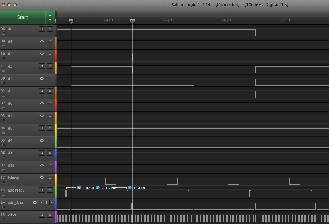
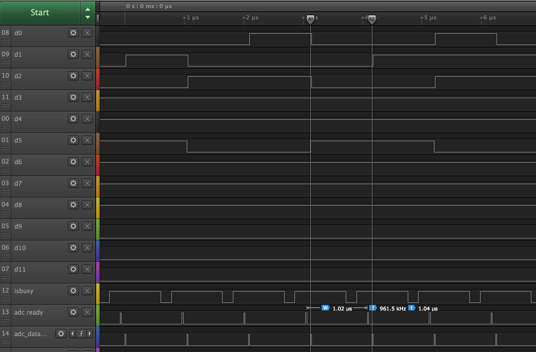
Data Acquisition (DAQ)
Back to top
Python
Python Installation on Windows

Python Code (serial1.py)
from tkinter import *
import serial
import serial.tools.list_ports
import codecs
import time

root = Tk()
These lines of code bring the right packages in, and since we will be using
Python in an object oriented way, the last line defines the name of the
main object. The line "from tkinter import *" means import all libraries
related to the TCL GUI library we downloaded (see above). The next 4
loads the Python serial interface, some special tools used to get the list of
COM ports we can open, some codecs to convert from/to Unicode, and a library
to allow you to find out the time.
# create the main window
def main():

    # modify the window
    root.title("Serial Port Communication")
    root.wm_title("Serial Port Communication")
    root.geometry("500x500+800+400")
    root.update()

    #create the frame that holds other widgets
    app = Application(root)

    #kick off event loop
    root.mainloop()

    #call main() to get things going
if __name__ == '__main__':
    main()
Most of what this code does is to define a thing called "main(), which does the following:
Since "def main():" starts on the 1st column, the line "if __name__..." ends the definition
of the code in main(). That line uses the name '__main__', checks whether it's equal to
"'__main__'", and if it is, invokes the code in "main()". This is a bit convoluted, you
could probably also have just simple said "main()" in the first column. However it's safer
to do it this way, because a module’s __name__ is set equal to '__main__' when read
from standard input, a script, or from an interactive prompt, which describes what we are
doing. So this line tells Python that
if we are in the main loop (which we are), then call the object main() that
we made when we did "def main():".
class Application(Frame):
    """ Create the window and populate with widgets """

    def __init__(self,parent):
        """ initializes the frame """
        Frame.__init__(self,parent,background="white")
        self.parent = parent
        self.grid()
        self.create_widgets()
        self.isopen = 0
The arguments "self" and "parent" point to objects so you can use them in the code to
follow. "Frame...." initializes the "Frame", a concept sort of equivalent to defining
regions inside the main GUI where you can put widgets. You can use many Frames and
control the grid of widgets, but here we will just use one. The next line
"self.parent=parent" sets up a pointer to the "parent" object that hangs off the
"self" ("Application") structure. The next 2 lines call methods you will define below,
and "self.isopen = 0" defines a variable within the Applications object called "isopen",
and initializes it to 0. It will be set to 1 when we actually open a port, and this is
how the rest of the code will know (if it cares) whether a port is open.
        self.buttonQ = Button(self, text="Quit")
        self.buttonQ["command"] = self.quitit
        self.buttonQ.grid(row=0,column=0, sticky=W)

        self.buttonOP = Button(self,text="Open")
        self.buttonOP["command"] = self.openPort
        self.buttonOP.grid(row=0,column=1, sticky=W)

        self.buttonR = Button(self,text="Receive: ")
        self.buttonR.grid(row=0,column=2, sticky=W)
        self.buttonR["command"] = self.getdata

        self.buttonS = Button(self,text="Send Hex:")
        self.buttonS["command"] = self.senddata
        self.buttonS.grid(row=0,column=3,sticky=W)
        self.stext = Text(self,height=1,width=100)
        self.stext.grid(row=0,column=4)

        self.clabel = Label(self,text="Enter COMx port:")
        self.clabel.grid(row=1,column=0, columnspan=4, sticky=W)
        self.ctext = Text(self,height=1,width=6)
        self.ctext.grid(row=1,column=4, sticky=W)
        self.ctext.insert("1.0","COM4")

        self.blabel = Label(self,text="Enter baud (default=1,000,000): ")
        self.blabel.grid(row=2,column=0, columnspan=4,sticky=W)
        self.btext = Text(self,height=1,width=8)
        self.btext.grid(row=2,column=4, sticky=W)
        self.btext.insert("1.0","1000000")

        self.stlabel = Label(self,text="Status: ")
        self.stlabel.grid(row=3,column=0,  sticky=W)
        self.status = Text(self,height=100,width=100)
        self.status.grid(row=4, column=0, columnspan=5, sticky=W)
        self.status.delete("1.0",END)

#       parity = serial.PARITY_EVEN
#       stopbits = serial.STOPBITS_ONE

        #
        # list all the serial ports
        #
        ports = list(serial.tools.list_ports.comports())
        self.status.insert(END,"Available COM ports:\n")
        for p in ports:
            self.status.insert(END,p)
            self.status.insert(END,"\n")
#           print(p)
The first button will be called "buttonQ", and the intention is taht when you click it,
the application should exit. The code 'text="Quit"' is just
the text inside the button, and the next line tells it the callback
(which means when the button is clicked, invoke "quitit()". See below for the code
inside quitit.
The "grid" method tells it to put this button on row 0, column 1,
and "sticky=W" means left justify (amusingly, Python uses N/S and E/W
for Up/Down and Left/Right). Below that are more buttons, labels,
and text widgets (where you can write information and use to input
into the application).
#       parity = serial.PARITY_EVEN
#       stopbits = serial.STOPBITS_ONE
are commented out because we don't use them, but they are included just in case
we do need them sometime. At at the end the print line
# print(p)
is also commented out. What "print(string)" does is to print the "string"
onto the command line. This can be an effective way of debugging.
    def quitit(self):
        print("That's all folks!")
        quit()

    def openPort(self):
        if self.isopen == 1:
            self.status.insert(END,"Port is already open!\n")
            return

        port = self.ctext.get("1.0",END).strip('\n')
        sbaud = self.btext.get("1.0",END)
        baud = int(sbaud)
#       print("port="+port+"  baud="+sbaud)
        self.ser = serial.Serial(port,sbaud,timeout=1)
        if self.ser.isOpen():
            self.status.insert(END,self.ser.name + " is now open\n")
#           print(self.ser.name + " is now open...")
            self.isopen = 1
        else:
            self.status.insert(END,self.ser.name + " is NOT open!!!\n")
#           print("sorry, problem trying to open port "+port+"\n")
"quitit()" is connected to the "Quit" button "buttonQ", and all it does is
printout a text message "That's all folks!" to the console, and quit by calling
the Python function "quit()".
"openPort()" is connected to the "Open" button "buttonOP". You can see
what the code does: it first checks if it's already opened a port, and if so it
types "Port is already open!" with a "return" ("\n") to the status text object
(see self.status in the code create_widgets() above). It then grabs the
port (which COM port from the ctext widget), and the baud rate, and makes the
connection self.ser, which is filled by using the serial.Serial method.
Note that the "serial" part of "serial.Serial" is the handle to all of the serial
port calls as defined at the top via "import serial". The "Serial" part is the
method to the "serial" object that makes the connection. It then checks if
the method is successful by looking at the method self.ser.isOpen(), which is a
logical (true/false). If it's true, then it reports everything is ok, sets
self.isopen to 1, and that's it. If it does not open ok, it reports that and
exits.
    def getdata(self):
        #
        # check to see if any port has been opened or not
        #
        if self.isopen == 0:
            self.status.insert(END,"Sorry but you MUST open a port first!")
            return
        #
        # now wait for input
        #
        sleep_time = 0.1
        nbytes = 1
        noinput = 1
        self.status.insert(END,"Waiting...")
        root.update_idletasks()
        while noinput == 1:
            tdata = self.ser.read(nbytes)
            ld = len(tdata)
#           print(ld)
            if ld > 0:
                #
                # flag input has arrived and print out in hex
                #
                noinput = 0
#               print(tdata)
                udata = hex(int.from_bytes(tdata,byteorder="little"))
                self.status.insert(END,"\nOk, data received, saw this in hex: "+udata+"\n")
            else :
                #
                # no input - sleep for some number of seconds and try again
                #
                time.sleep(sleep_time)
                self.status.insert(END,".")
                root.update_idletasks()
The first thing it does is check if the COM port is not open, and if not
complains by inserting the phrase "Sorry but you MUST open a port first!"
into the last row ("END") of the text widget "self.status". This keeps the program
from crashing if you try to get data before opening a port. It then goes into
a loop where it checks to see if the python serial receiver saw anything, and
if not sleeps for some amount of time, in seconds, as specified in the variable
"sleep_time", before checking again. We will use a default of 0.1 sec for this
wait period. This is an infinite loop,
so it will wait forever. You could easily insert a counter and implement a
timeout.
    def senddata(self):
        #
        # check to see if any port has been opened or not
        #
        if self.isopen == 0:
            self.status.insert(END,"Sorry but you MUST open a port first!\n")
            return
        #
        # decode stext as a hex string, but first strip off the \n and convert to uppercase
        # if the string is blank, send 00.  if it's 1 digit, pad a 0 (e.g. "1" -> "01")
        #
        cmd = self.stext.get("1.0",END).strip('\n').upper()
        lcmd = len(cmd)
        if lcmd == 0:
            cmd = "00"
        if lcmd == 1:
            cmd = "0" + cmd
        hcmd = bytearray.fromhex(cmd)
#       print (hcmd + cmd)
        self.status.insert(END,"sending "+cmd+"...\n")
        self.ser.write(hcmd)
Running Python Serial IO Script serial1.py
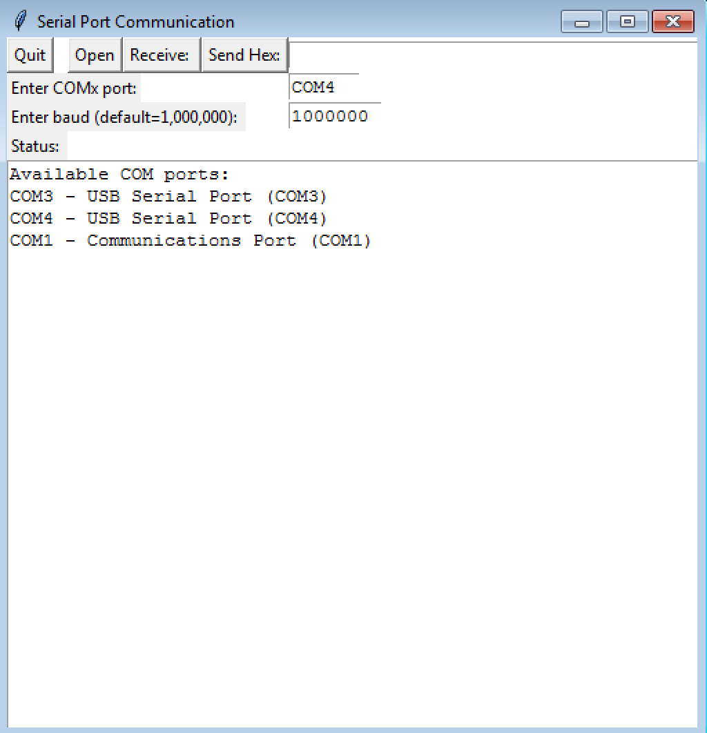
FPGA Voltmeter 2
The project voltmeter2 can be found in a zipped format
here. When you download this
project to the BASYS3 board and hit the upper button "btnU", you shoud
see "3008" as the version number on the LED digit display. To run operate this
project on the board, you hit "btnL" (left button) to latch 16 bits
of ADC value. Each time you latch it it will show the latched value
on the LED digit display. It will also show the upper 12 bits of the
ADC value continuously on the LEDs (the individual bank of 16 above
the switches).
This might seems like a
lot of waiting around for signals, but it is the most straight forward
way to be sure that the state machine is under control and doesn't
get into an illegal state. Remember, state machines respond to the
inputs, and it's always good if you are not in a rush to make things
as synchronous as possible. This kind of thing is called "hand shaking",
and makes the firmware as stable as can be as long as you have some
rules and follow them. The state machine is shown in the figure below.
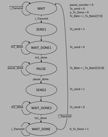
Voltmeter 2 Python code serial2.py
    def __init__(self,parent):
        """ initializes the frame """
        Frame.__init__(self,parent,background="white")
        self.parent = parent
        self.grid()
        self.create_widgets()
        self.isopen = 0
The line "self.grid()" sets up a grid inside "Frame", and each widget
specifies the row and column in that grid (along with columnspan as appropriate).
For "serial2.py", you will see the following new code
in the constructor method for Application(frame):
    def __init__(self,parent):
        """ initializes the frame """
        Frame.__init__(self,parent,background="white")
        self.isopen = 0
        self.Frame1 = Frame(parent)
        self.Frame1.grid(row=0, column=0, sticky="wens")
        self.Frame2 = Frame(parent)
        self.Frame2.grid(row=1, column=0, sticky="wens")
        self.parent = parent
        self.create_widgets()
Notice the 2 new variables "self.Frame1" and "self.Frame2". Each of these frames
will itself be a frame that the widgets will have to attach to. Frame1 is at
row=0, column=0 and frame 2 is at row=1, column=1.
    def create_widgets(self):
        self.buttonQ = Button(self.Frame1, text="Quit")
        self.buttonQ["command"] = self.quitit
        self.buttonQ.grid(row=0,column=0, sticky=W)

        self.buttonOP = Button(self.Frame1,text="Open")
        self.buttonOP["command"] = self.openPort
        self.buttonOP.grid(row=0,column=1, sticky=W)

        self.buttonR = Button(self.Frame1,text="Receive: ")
        self.buttonR.grid(row=0,column=2, sticky=W)
        self.buttonR["command"] = self.getdata

        self.buttonS = Button(self.Frame1,text="Send Hex:")
        self.buttonS["command"] = self.senddata
        self.buttonS.grid(row=0,column=3,sticky=W)
        self.stext = Text(self.Frame1,height=1,width=100)
        self.stext.grid(row=0,column=4)

        self.clabel = Label(self.Frame1,text="Enter COMx port:")
        self.clabel.grid(row=1,column=0, columnspan=4, sticky=W)
        self.ctext = Text(self.Frame1,height=1,width=6)
        self.ctext.grid(row=1,column=4, sticky=W)
        self.ctext.insert("1.0","COM4")

        self.blabel = Label(self.Frame1,text="Enter baud (default=1,000,000): ")
        self.blabel.grid(row=2,column=0, columnspan=4,sticky=W)
        self.btext = Text(self.Frame1,height=1,width=8)
        self.btext.grid(row=2,column=4, sticky=W)
        self.btext.insert("1.0","1000000")

        self.stlabel = Label(self.Frame1,text="Status: ")
        self.stlabel.grid(row=3,column=0,  sticky=W)
All of these widgets now attach to "Frame1" instead of "Frame".
        """ status is a text widget with it's own frame """

        self.status = Text(self.Frame2,height=30,width=60, relief="sunken")
        self.status.grid(row=0, column=1, columnspan=5, sticky=W)
        self.statusSB = Scrollbar(self.Frame2,command=self.status.yview, orient=VERTICAL)
        self.status['yscrollcommand'] = self.statusSB.set
        self.statusSB.grid(row=0,column=0, sticky="nsew")
        self.status.delete("1.0",END)
You can see here that the status text widget attaches to row=0 and
column=1 of "Frame2", and we add a Scrollbar called "self.statusSB" to
row=0 and column=0 of the same "Frame2". The rest of the code sets up
the scroll bar as controlling the "self.status" widgets so that you can
scroll up and down after many measurements. Note that the height of
status is now set as "height=30", which means it will show 30 lines.
If you have more than that then the scrollbar allows you to scroll.
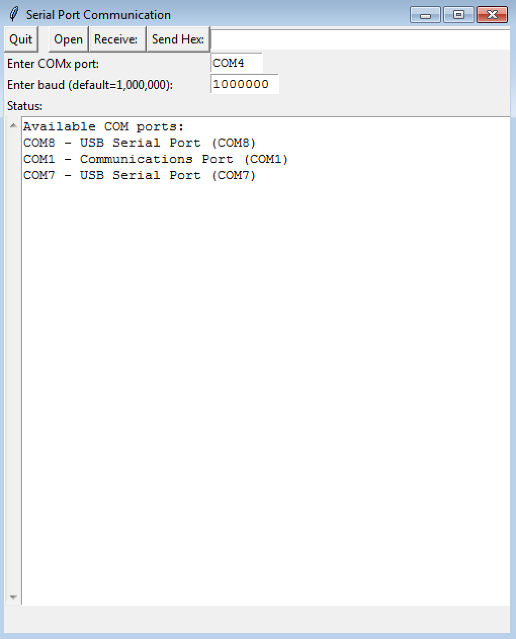
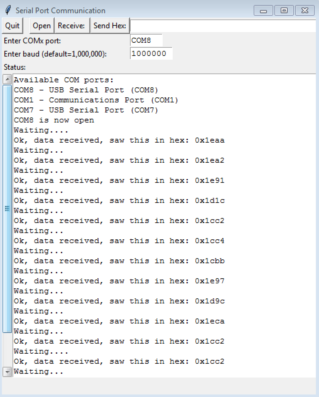
A Real FPGA Voltmeter
The code for the state machine inside top.v is shown below:
reg sendit;
wire tx_done, tx_ready;
reg [15:0] every_n;
always @ (posedge clk20) begin
    if (reset) begin
        sendit <= 0;
        every_n <= 0;
        adc_state <= WAIT;
        latched_adc <= 0;
    end
    else case (adc_state)
        WAIT: begin
            //
            // watch for btnL or btnD to signal we want to latch something
            //
            every_n <= 0;
            sendit <= 0;
            if (onoff) adc_state <= LATCH;
            else adc_state <= WAIT;
            end
        LATCH: begin
            //
            // latch it
            //
            every_n <= every_n + 1;
            if (every_n == sw) begin
                latched_adc <= r_adc_data;
                adc_state <= SENDIT;
                end
            else adc_state <= LATCH;
            end
        SENDIT: begin
            //
            // wait for the button to no longer be pushed
            //
            sendit <= 1;
            adc_state <= WAIT_END;
            end
        WAIT_END: begin
            sendit <= 0;
            if (tx_done) adc_state <= WAIT;
            else adc_state <= WAIT_END;
            end
        default: begin
            sendit <= 0;
            every_n <= 0;
            adc_state <= WAIT;
            end
    endcase
    end
And the state machine diagram is in the figure below:
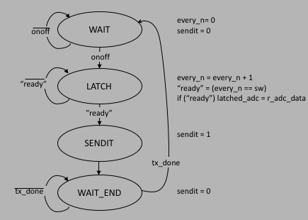
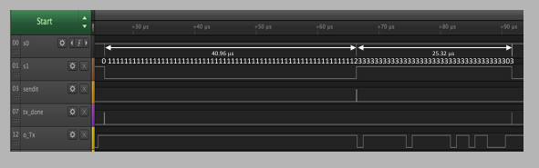
The zipped project can be found
here
Continuous Voltmeter Python code
The Python code to turn display a voltage continuous can be found
here. The highlights are:
When you run the script "voltmeter.py" you should see the following:
Pulse Width Modulation (PWM)
Back to top
`timescale 1ns / 1ps

module top(
    input clk,
    input sw0,
    output [15:0] led
    );

    //
    // make a 14 bit counter to turn on and off all 16 LEDs with different pulse widths
    //
    reg [13:0] counter;
    always @ (posedge clk) counter <= counter + 1;
    //
    assign led[15:0] = {counter[13:0],clk,sw0};
endmodule
The statement "assign led[15:0] = {counter[13:0],clk,sw0};" is called a
Verilog "concatenation", and is actually 16 statements in one. The
assignment says that we want to connect led[15] to counter[13], then
led[14] to counter[12], and so on down to led[1] connected to clk and
led[0] connected to sw0.
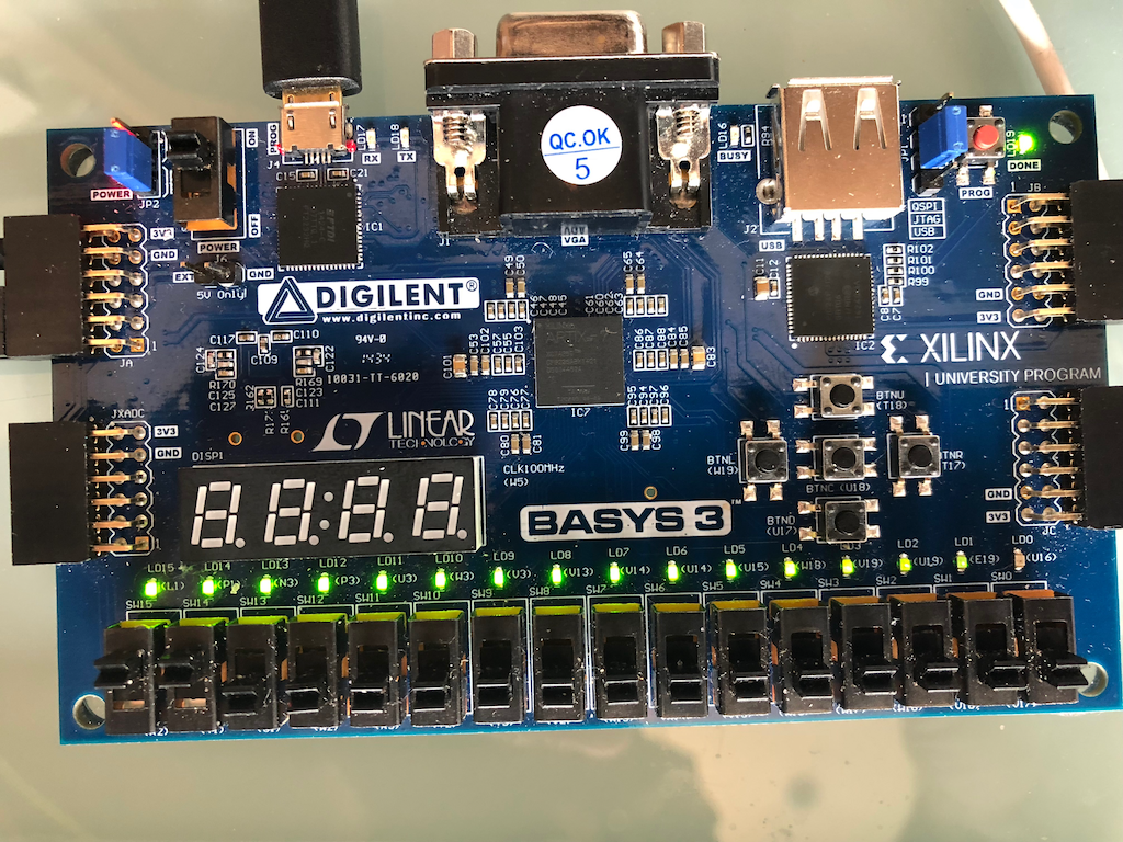
Changing the Duty Factor

module top(
    input clk,
    input [15:0] sw,
    input btnU,             // reset
    output [15:0] led
    );

    //
    // turn the FSM on using sw[15];
    //
    wire enable = sw[15];
    //
    // let's say we want 1024 times the clock period for period of the output signal
    //
    // for the ON and OFF registers, we will use the bottom 10 switches.
    // so full scale 100% duty factor will be ON='h3FF and OFF = 0, so the calculation
    // we need is:
    //
    wire [9:0] on, off;
    assign on = sw[9:0];
    assign off = 'h3FF - on;
    //
    // now make the counters and the output and the FSM
    //
    reg [9:0] count_on, count_off;
    reg OUT;
    localparam [1:0] WAIT=0, ON=1, OFF=2;
    reg [1:0] state;
    always @ (posedge clk)
        if (btnU) begin
            state <= WAIT;
            OUT <= 0;
        end
        else case (state)
            WAIT: begin
                OUT <= 0;
                count_on <= 0;
                count_off <= 0;
                if (enable) state <= ON;
                else state <= WAIT;
            end
            ON: begin
                OUT <= 1;
                count_off <= 0;
                count_on <= count_on + 1;
                if (count_on == on) state <= OFF;
                else state <= ON;
            end
            OFF: begin
                OUT <= 0;
                count_on <= 0;
                count_off <= count_off + 1;
                if (count_off == off) begin
                    if (enable) state <= ON;
                    else state <= WAIT;
                    end
                else state <= OFF;
            end
            default: begin
                OUT <= 0;
                count_on <= 0;
                count_off <= 0;
                state <= WAIT;
            end
        endcase
    //
    // now drive the output onto led[15], and have the lower 10 led's follow the switches
    //
    assign led = {OUT,5'b00000,on[9:0]};
endmodule
Switch sw[15] turns the thing on (wire enable = sw[15]), and we have made the
register busses be 10 bits wide, which means our pulse will be $1024\times 10ns = 10.24\mu s$
wide. Note that in the code, we set the on and off registers so that the sum adds
up to 10'h3FF = 1023 decimal. The value for on comes from the bottom 10 switches, and
off is set to 10'h3FF-off. For a 50% duty factor, you would set on = 512 decimal
(turn on all 9 bottom switches).
Modulating the Duty Factor
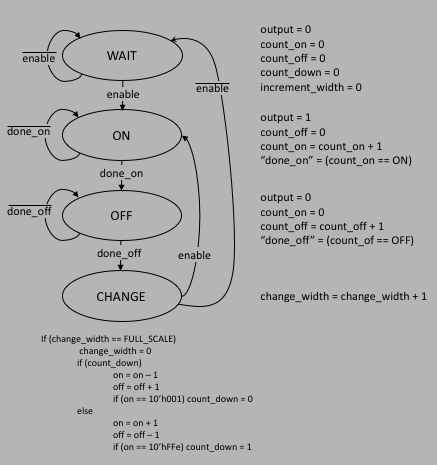
`timescale 1ns / 1ps
module top(
    input clk,
    input [15:0] sw,
    input btnU,             // reset
    output [15:0] led
    );

    //
    // turn the FSM on using sw[15];
    //
    wire enable = sw[15];
    //
    // let's say we want 1024 times the clock period for period of the output signal
    //
    // for the "on" and "off" registers, we will modulate them using a large register.
    // so full scale 100% duty factor will be ON='h3FF and OFF = 'h0
    //
    // now make the counters and the output and the FSM
    //
    reg [9:0] count_on, count_off;
    reg OUT;
    reg [9:0] on, off;
    reg [7:0] change_width;
    wire [7:0] sw8 = sw[7:0];
    wire [7:0] beats = (sw8 == 8'h0 ? 8'hFF : sw8);
    reg count_down;         // 0=increment, 1=decrement
    localparam [1:0] WAIT=0, ON=1, OFF=2, CHANGE=3;
    reg [1:0] state;
    always @ (posedge clk)
        if (btnU) begin
            state <= WAIT;
            OUT <= 0;
            on <= 0;
            off <= 'hFFFF;
            change_width <= 0;
            count_down <= 0;
        end
        else case (state)
            WAIT: begin
                OUT <= 0;
                count_on <= 0;
                count_off <= 0;
                on <= 0;
                count_down <= 0;
                change_width <= 0;
                if (enable) state <= ON;
                else state <= WAIT;
            end
            ON: begin
                OUT <= 1;
                count_off <= 0;
                count_on <= count_on + 1;
                if (count_on == on) state <= OFF;
                else state <= ON;
            end
            OFF: begin
                OUT <= 0;
                count_on <= 0;
                count_off <= count_off + 1;
                if (count_off == off) state <= CHANGE;
                else state <= OFF;
            end
            CHANGE: begin
                //
                // in this state we check to see if it's
                // time to change the on/off %
                //
                change_width <= change_width + 1;
                if (change_width == beats) begin
                    change_width <= 0;
                    if (count_down) begin
                        on <= on - 1;
                        off <= off + 1;
                        if (on == 10'h001) count_down <= 0;
                    end
                    else begin
                        on <= on + 1;
                        off <= off - 1;
                        if (on == 10'h3FE) count_down <= 1;
                    end
                 end
                 if (enable) state <= ON;
                 else state <= WAIT;
            end
            default: begin
                count_on <= 0;
                count_off <= 0;
                on <= 0;
                count_down <= 0;
                change_width <= 0;
                state <= WAIT;
            end
        endcase
    //
    // now drive the output onto led[15]
    //
    assign led = {OUT,5'h0,on[9:0]};
endmodule
With the above code, and a 10ns clock, we would need 10 bits (1024) ticks
for each value of the "on" and "off" register. So the LED will have a
constant brightness for $10ns \times 1024 = 10.24\mu s$.
Then, we change each value according to an 8-bit register, and if we want
to use full scale, that it will take $256\times 10.24\mu s = 2.62ms$ for the
LED to brightness. Using all 10 bits of the "on" register, it will take
$1024\times 2.62ms = 2.68s$ to turn on and an equivalent time to turn off.
That means the "heartbeat" will beat once every 5.4s. If we want to speed
that up, we would set the
bit switches accordingly, so that the "on" and "off" registers change after
a smaller amount of time. So if we put the switches at 0x40 (all are off
except for bit 6), then we will speed up the hearbeat by x4, or once every
$1.1s$.

Waveform Generator
Back to top

`timescale 1ns / 1ps

module top(
    input clk,
    input [15:0] sw,
    input btnU,             // reset
    output [15:0] led,
    output wave,            // this drives the RC circuit and is same as OUT
    output wave2,           // also same as OUT but free of RC circuit
    output reg pulse,        //
    output reg count_down    // 0=increment, 1=decrement
    );

    //
    // turn the FSM on using sw[15];
    //
    wire enable = sw[15];
    //
    // let's say we want 1024 times the clock period for period of the output signal
    //
    // for the "on" and "off" registers, we will modulate them using a large register.
    // so full scale 100% duty factor will be ON='h3FF and OFF = 0, so the calculation
    // we need is:
    //
    //
    // now make the counters and the output and the FSM
    //
    reg [10:0] count_on, count_off;
    reg [10:0] on, off;
    wire [10:0] width_on, width_off;
    parameter [10:0] FULL = 11'h7FE;
    parameter [10:0] START = 11'h001;
    reg OUT;
    reg [4:0] change_width;
    //
    // "beats" is the value of the counter that determines how long the duty cycle
    // is constant
    //
    wire [4:0] sw8 = sw[4:0];
    wire [4:0] beats = (sw8 == 5'h0 ? 5'h1F : sw8);
    localparam [1:0] WAIT=0, ON=1, OFF=2, CHANGE=3;
    reg [1:0] state;
    always @ (posedge clk)
        if (btnU) begin
            state <= WAIT;
            OUT <= 0;
            on <= START;
            off <= FULL;
            change_width <= 0;
            count_down <= 0;
            pulse <= 0;
        end
        else case (state)
            WAIT: begin
                OUT <= 0;
                count_on <= 0;
                count_off <= 0;
                on <= START;
                off <= FULL;
                count_down <= 0;
                change_width <= 0;
                pulse <= 0;
                if (enable) state <= ON;
                else state <= WAIT;
            end
            ON: begin
                OUT <= 1;
                count_off <= 0;
                count_on <= count_on + 1;
                if (count_on == on) state <= OFF;
                else state <= ON;
            end
            OFF: begin
                OUT <= 0;
                count_on <= 0;
                count_off <= count_off + 1;
                if (count_off == off) state <= CHANGE;
                else state <= OFF;
            end
            CHANGE: begin
                //
                // in this state we check to see if it's time to change the on/off percentage
                //
                change_width <= change_width + 1;
                if (change_width == beats) begin
                    change_width <= 0;
                    if (count_down) begin
                        on <= on - 1;
                        off <= off + 1;
                        if (on == START) begin
                            pulse = ~pulse;
                            count_down <= 0;
                        end
                    end
                    else begin
                        on <= on + 1;
                        off <= off - 1;
                        if (on == FULL) count_down <= 1;
                    end
                 end
                 if (enable) state <= ON;
                 else state <= WAIT;
            end
            default: begin
                count_on <= 0;
                count_off <= 0;
                on <= 0;
                count_down <= 0;
                change_width <= 0;
                state <= WAIT;
            end
        endcase
    //
    // now drive the output onto led[15]
    //
    assign led = {OUT,9'h0,on[5:0]};
    assign wave = OUT;
    assign wave2 = OUT;
endmodule
The pinouts (.xdc file) will look like this:
## This file is a general .xdc for the Basys3 rev B board
## To use it in a project:
## - uncomment the lines corresponding to used pins
## - rename the used ports (in each line, after get_ports) according to the top level signal names in the project

## Clock signal
set_property PACKAGE_PIN W5 [get_ports clk]
set_property IOSTANDARD LVCMOS33 [get_ports clk]
create_clock -period 10.000 -name sys_clk_pin -waveform {0.000 5.000} -add [get_ports clk]

# wave output
set_property PACKAGE_PIN J1 [get_ports wave]
set_property IOSTANDARD LVCMOS33 [get_ports wave]
set_property PACKAGE_PIN L2 [get_ports wave2]
set_property IOSTANDARD LVCMOS33 [get_ports wave2]
set_property PACKAGE_PIN J2 [get_ports pulse]
set_property IOSTANDARD LVCMOS33 [get_ports pulse]
set_property PACKAGE_PIN G2 [get_ports count_down]
set_property IOSTANDARD LVCMOS33 [get_ports count_down]


# LEDs
set_property PACKAGE_PIN U16 [get_ports {led[0]}]
set_property IOSTANDARD LVCMOS33 [get_ports {led[0]}]
set_property PACKAGE_PIN E19 [get_ports {led[1]}]
set_property IOSTANDARD LVCMOS33 [get_ports {led[1]}]
set_property PACKAGE_PIN U19 [get_ports {led[2]}]
set_property IOSTANDARD LVCMOS33 [get_ports {led[2]}]
set_property PACKAGE_PIN V19 [get_ports {led[3]}]
set_property IOSTANDARD LVCMOS33 [get_ports {led[3]}]
set_property PACKAGE_PIN W18 [get_ports {led[4]}]
set_property IOSTANDARD LVCMOS33 [get_ports {led[4]}]
set_property PACKAGE_PIN U15 [get_ports {led[5]}]
set_property IOSTANDARD LVCMOS33 [get_ports {led[5]}]
set_property PACKAGE_PIN U14 [get_ports {led[6]}]
set_property IOSTANDARD LVCMOS33 [get_ports {led[6]}]
set_property PACKAGE_PIN V14 [get_ports {led[7]}]
set_property IOSTANDARD LVCMOS33 [get_ports {led[7]}]
set_property PACKAGE_PIN V13 [get_ports {led[8]}]
set_property IOSTANDARD LVCMOS33 [get_ports {led[8]}]
set_property PACKAGE_PIN V3 [get_ports {led[9]}]
set_property IOSTANDARD LVCMOS33 [get_ports {led[9]}]
set_property PACKAGE_PIN W3 [get_ports {led[10]}]
set_property IOSTANDARD LVCMOS33 [get_ports {led[10]}]
set_property PACKAGE_PIN U3 [get_ports {led[11]}]
set_property IOSTANDARD LVCMOS33 [get_ports {led[11]}]
set_property PACKAGE_PIN P3 [get_ports {led[12]}]
set_property IOSTANDARD LVCMOS33 [get_ports {led[12]}]
set_property PACKAGE_PIN N3 [get_ports {led[13]}]
set_property IOSTANDARD LVCMOS33 [get_ports {led[13]}]
set_property PACKAGE_PIN P1 [get_ports {led[14]}]
set_property IOSTANDARD LVCMOS33 [get_ports {led[14]}]
set_property PACKAGE_PIN L1 [get_ports {led[15]}]
set_property IOSTANDARD LVCMOS33 [get_ports {led[15]}]

## Switches
set_property PACKAGE_PIN V17 [get_ports {sw[0]}]
set_property IOSTANDARD LVCMOS33 [get_ports {sw[0]}]
set_property PACKAGE_PIN V16 [get_ports {sw[1]}]
set_property IOSTANDARD LVCMOS33 [get_ports {sw[1]}]
set_property PACKAGE_PIN W16 [get_ports {sw[2]}]
set_property IOSTANDARD LVCMOS33 [get_ports {sw[2]}]
set_property PACKAGE_PIN W17 [get_ports {sw[3]}]
set_property IOSTANDARD LVCMOS33 [get_ports {sw[3]}]
set_property PACKAGE_PIN W15 [get_ports {sw[4]}]
set_property IOSTANDARD LVCMOS33 [get_ports {sw[4]}]
set_property PACKAGE_PIN V15 [get_ports {sw[5]}]
set_property IOSTANDARD LVCMOS33 [get_ports {sw[5]}]
set_property PACKAGE_PIN W14 [get_ports {sw[6]}]
set_property IOSTANDARD LVCMOS33 [get_ports {sw[6]}]
set_property PACKAGE_PIN W13 [get_ports {sw[7]}]
set_property IOSTANDARD LVCMOS33 [get_ports {sw[7]}]
set_property PACKAGE_PIN V2 [get_ports {sw[8]}]
set_property IOSTANDARD LVCMOS33 [get_ports {sw[8]}]
set_property PACKAGE_PIN T3 [get_ports {sw[9]}]
set_property IOSTANDARD LVCMOS33 [get_ports {sw[9]}]
set_property PACKAGE_PIN T2 [get_ports {sw[10]}]
set_property IOSTANDARD LVCMOS33 [get_ports {sw[10]}]
set_property PACKAGE_PIN R3 [get_ports {sw[11]}]
set_property IOSTANDARD LVCMOS33 [get_ports {sw[11]}]
set_property PACKAGE_PIN W2 [get_ports {sw[12]}]
set_property IOSTANDARD LVCMOS33 [get_ports {sw[12]}]
set_property PACKAGE_PIN U1 [get_ports {sw[13]}]
set_property IOSTANDARD LVCMOS33 [get_ports {sw[13]}]
set_property PACKAGE_PIN T1 [get_ports {sw[14]}]
set_property IOSTANDARD LVCMOS33 [get_ports {sw[14]}]
set_property PACKAGE_PIN R2 [get_ports {sw[15]}]
set_property IOSTANDARD LVCMOS33 [get_ports {sw[15]}]

##Buttons
set_property PACKAGE_PIN T18 [get_ports btnU]
set_property IOSTANDARD LVCMOS33 [get_ports btnU]
The full archived project can be found
here.
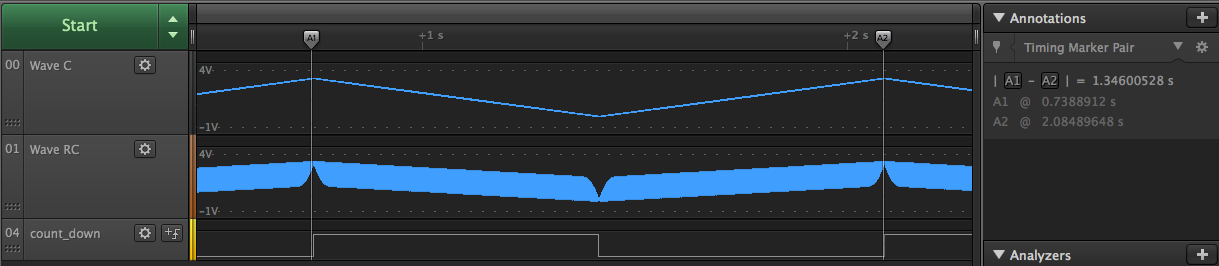
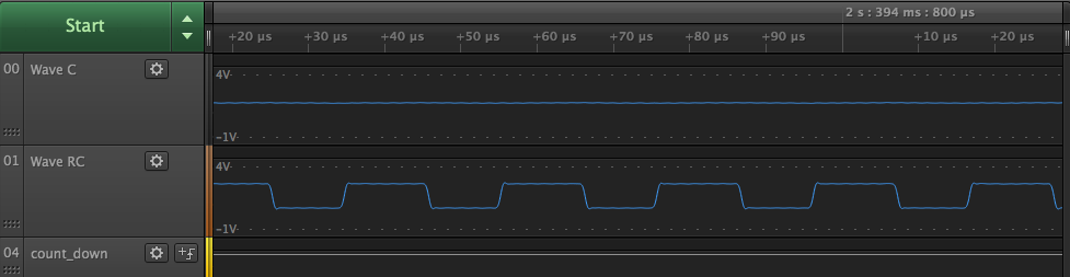
Auto Correlation
Back to top
Drew Baden
Last update May 24, 2018